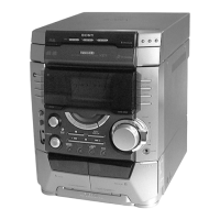
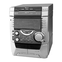
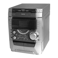
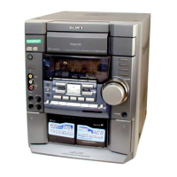
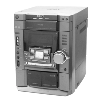
HCD-VX3A
24 24
IC101 @∞ MDP
1
2
3
4
Waveforms
CD SECTION
IC101 %º RFAC
IC101 $¡ TE
IC101 #ª FE
1.3Vp-p
APPROX 500mVp-p
2.5V
APPROX 200mVp-p
2.5V
2.6Vp-p
7.5µsec
1
2
3
IC505 &∞ COUT
IC505 ^ª YOUT
4
5
6
7
8
9
IC509 !¶ BCLK
IC509 !ª LRCK
0
!¡
!™
IC502 !£ XOUT
4Vp-p
10MHz
IC401 7 COUT
IC401 1 YOUT
J302 VOUT
IC509 1 XT1
27MHz
5.8Vp-p
4.6Vp-p
44.1kHz
4.8Vp-p
2.11MHz
IC504 8 384FS
4.8Vp-p
33.8MHz
IC504 6 27M
3.8Vp-p
27MHz
2.8Vp-p
33.8MHz
IC504 !™
VIDEO SECTION
H
1Vp-p
H
1Vp-p
2Vp-p
H
2Vp-p
H
H
1.2
Vp-p
THIS NOTE IS COMMON FOR PRINTED WIRING
BOARDS AND SCHEMATIC DIAGRAMS.
(In addition to this, the necessary note is printed
in each block.)
For schematic diagrams.
Note:
• All capacitors are in µF unless otherwise noted. pF: µµF
50 WV or less are not indicated except for electrolytics
and tantalums.
• All resistors are in Ω and
1
/
4
W or less unless otherwise
specified.
•
¢
: internal component.
• 2 : nonflammable resistor.
• 1 : fusible resistor.
• C : panel designation.
For printed wiring boards.
Note:
• X : parts extracted from the component side.
• Y : parts extracted from the conductor side.
• p : parts mounted on the conductor side.
•
®
: Through hole.
• b : Pattern from the side which enables seeing.
(The other layers' patterns are not indicated.)
• U : B+ Line.
• V : B– Line.
• H : adjustment for repair.
• Voltages and waveforms are dc with respect to ground
under no-signal (detuned) conditions.
• Voltages are taken with a VOM (Input impedance 10 MΩ).
Voltage variations may be noted due to normal produc-
tion tolerances.
• Waveforms are taken with a oscilloscope.
Voltage variations may be noted due to normal produc-
tion tolerances.
• Circled numbers refer to waveforms.
• Signal path.
F : FM
g : VIDEO/MD
E : PB (DECK A)
d : PB (DECK B)
G : REC (DECK B)
m : CHROMA
n : Y
o : VIDEO
J : CD
c : digital out
• Abbreviation
EA : Saudi Arabia model
MY : Malaysia model
SP : Singapore model
IA : Indonesia model
TH : Thai model
TW : Taiwan model
JE : Tourist model
Note: The components identified by mark ! or dotted line
with mark ! are critical for safety.
Replace only with part number specified.
• Indication of transistor
C
These are omitted
EB
Caution:
Pattern face side: Parts on the pattern face side seen from the
(Side B) pattern face are indicated.
Parts face side: Parts on the parts face side seen from the
(Side A) parts face are indicated.
Q
C
These are omitte