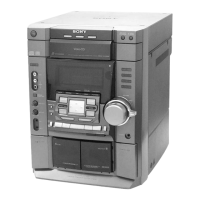
52
Pin No. Pin Name I/O Description
1 DVDD0 — Digital power supply
2 XRST I System reset
3 MUTE I Muting selection pin
4 DATA I Serial data input, supplied from CPU
5 XLAT I Latch input, supplied from CPU
6 CLOK I Serial data transfer clock input, supplied from CPU
7 SENS O SENS output
8 SCLK I SENS serial data read-out clock
9 ATSK I/O Input pin for anti-shock (Ground)
10 WFCK O WFCK (Write Frame Clock) output (Not used)
11 XUGF O XUGF output (Not used)
12 XPCK O XPCK output (Not used)
13 GFS O GFS output (Not used)
14 C2P0 O C2PO output
15 SCOR O Sub-code sync output
16 CM4 O 4.2336MHz output (Not used)
17 WDCK O 48-bit slot D/A interface word clock (Not used)
18 DVSS — Digital ground
19 COUT O Numbers of track counted signal output (Not used)
20 MIRR O Mirror signal output (Not used)
21 DFCT O Defect signal output (Not used)
22 FOK O Focus OK output (Not used)
23 PWM1 I (Not used)
24 LOCK I/O GFS in sampled by 460Hz (Not used)
25 MDP O Output to control spindle motor servo
26 SSTP I Input signal to detect disc inner most trak
27 FST0 O 2/3 divider output (Not used)
28 DVDD1 — Digital power supply
29 SFDR O
Sled drive output
30 SRDR O
31 TFDR O
Tracking drive output
32 TRDR O
33 FFDR O
Focus drive output
34 FRDR O
35 DVSS1 — Digital ground
36 TEST I
TEST pin connected normally ground
37 TES1 I
38 VC I Center voltage input
39 FE I FOCUS error signal input
40 SE I Sled error signal input
• BD BOARD IC101 DIGITAL SIGNAL PROCESSOR (CXD3008Q)