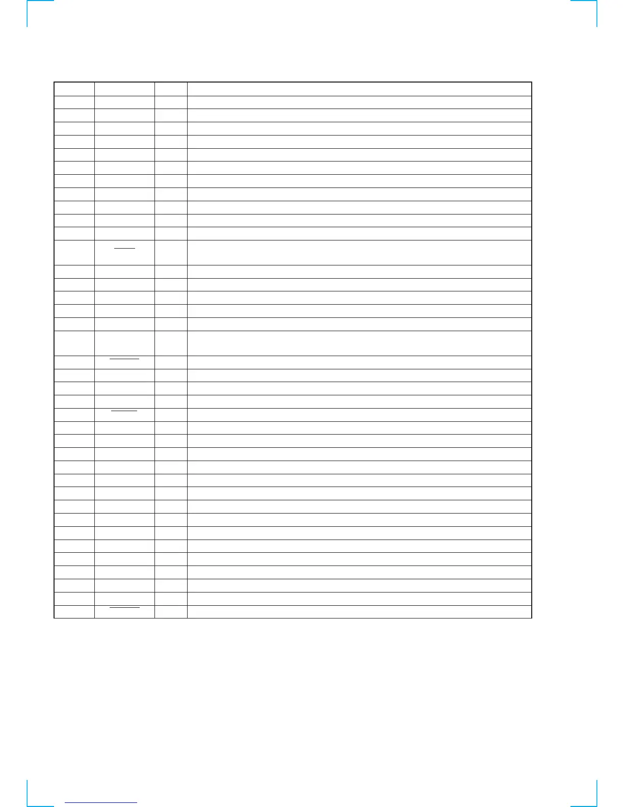
68
Pin No.
1
2
3
4
5
6
7
8
9
10
11
12
13
14
15
16
17
18
19
20
21
22
23
24 to 30
31
32
33
34
35
36
37
38 to 47
48
49
50
51
52
53
I/O
I
I
O
O
I
I
I
I
—
I
O
I
O
—
I
—
I
I
I
I
I
I
O
O
O
I
O
O
O
I
O
O
I
I
I
I
I
O
Description
Jog dial pulse input from rotary encoder (S713 lAMSL) (phase B input)
Jog dial pulse input from rotary encoder (S713 lAMSL) (phase A input)
C1 error rate output during test mode (Blank terminal)
ADER output during test mode (Blank terminal)
Sub code Q sync (SCOR) input from CXD2656R (IC121) Input “L” every 13.3 msec “H” is input mostly
Remote control receiving signal input form remote control receiver (IC761)
SIRCS remote control signal input for the S-LINK control A1
Input terminal to select the external data bus width. “L: 16 bit, “H”: 8 bits. (Fixed at “L”)
Ground
Sub system clock input (32.768 kHz)
Sub system clock input (32.768 kHz)
System reset signal input from reset signal generator (IC240) “L”: Reset.
Input “L” during the several 100 ms after the power startup then change to the “H” input
Main system clock output (7 MHz)
Ground
Main system clock input (7 MHz)
Power supply (+3.3 V)
Non-maskable interrupt input terminal. Fixed at “H”)
Sub code Q sync (SCOR) input of digital-in U-bit CD format from CXD2656R (IC121)
Input “L” every 13.3 msec “H” is input mostly
Power down detection input. Input “L” when power down is detected
Interrupt status input from CXD2656R (IC121)
Jog dial pulse input from rotary encoder (S740 REC LEVEL DEGITAL) (phase B input)
Jog dial pulse input from rotary encoder (S740 REC LEVEL DEGITAL) (phase A input)
Reset signal output to A/D converter (IC302) “L”: Reset
Not used in this system (Blank terminal)
Write data output to CXD2656R (IC121) and CXD8762Q (IC501)
Read data input from CXD2656R (IC121)
Serial clock signal output to CXD2656R (IC121) and CXD8762Q (IC501)
Chip select signal output to fluorescent display tube/LED drive IC (IC771) “L”: Active
Serial data output for display to fluorescent display tube/LED drive IC (IC771)
Not used in this system (Fixed at “L”)
Serial data transfer clock signal output for display to fluorescent display tube/LED drive IC (IC771)
Not used in this system (Blank terminal)
Initial data input terminal for the watch setting in local time. Fixed to “H”
Initial data input terminal for the watch setting in local time. Fixed to “H”
Initial data input terminal for the loading control method. “H”: IN switch is not used. (Fixed at “H”)
Not used in this system (Fixed at “L”)
Busy monitor signal input from CXD2656R (IC121)
Reset signal output to CXD2656R (IC121), BH6511FS (IC152), CXD8512Q (IC301) “L”: Reset
Pin Name
JOG1
JOG0
C1ERO
ADERO
SQSY
RMC
A1IN
BYTE
CNVSS
XIN-T
XOUT-T
S.RST
XOUT
GND
XIN
+ 3.3 V
NMI
DQSY
P.DOWN
XINT
DVOL1
DVOL0
ADRST
NC
SWDT
SRDT
SCLK
FLCS
FLDATA
NC
FLCLK
NC
CSET0
CSET1
20/X720
NC
MNT2 (XBUSY)
DIG-RST
• AD BOARD IC800 M30624MG-215FP (SYSTEM CONTROLLER)
 Loading...