46
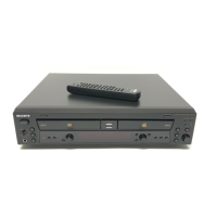
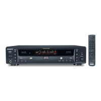
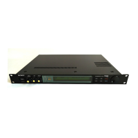
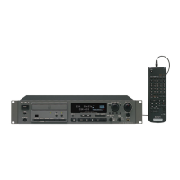
RCD-W3
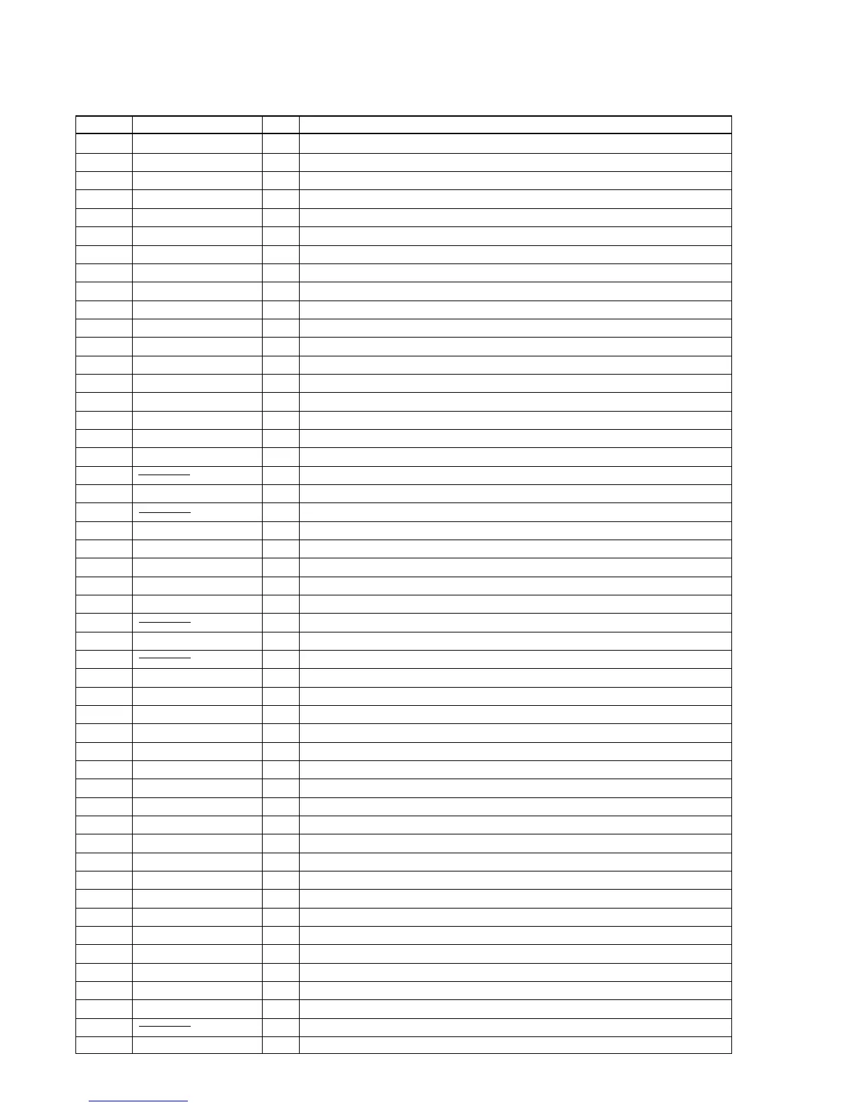
Pin No. Description
• IC407 HD64F3062BFBL-W3CDP (SYSTEM CONTROL) (BD-R Board (6/6))
1 VCL — Power supply (Connected to ground with capacitor)
2 DAC CS O DAC chip select signal output to FPGA (VC0IS05)
3 SW O Mode switching signal output to CXA2581N
4 CXA VFC O EQ cut-off frequency control signal output to CXA2581N
5 TRAYCTRL O TRAY loading motor control signal output to M63021FP
6 TRK INC O TRK INC signal output to CD-RW system control
7 SW REF/AUD O Audio level /sled reference voltage select signal output
8 FPGA AS O Register Control signal output to FPGA (VC0IS05)
9 DRV MUTE O Motor drive muting signal output to M63021FP
10 FW EN I Flash write enable signal input
11 GND — Ground
12 AS DATA O Serial communication with CD-RW data output/ASIC config
13 FL SDI O FLD data out/flash write
14 REC TXD I Serial communication with CD-RW data input/ASIC config
15 PROG DN I Flash read input
16 AS CLK O Not used (open)
17 FL SCK O FLD clock output
18 FL CE O FLD chip enable signal output
19 — Not used (open)
20 FPGA RST O Reset signal output to FPGA (VC0IS05)
21 — Not used (open)
22 GND — Ground
23 FPGA DATA I/O FPGA serial data input/output
24 FPGA CLK I/O FPGA clock input/output
25 FPGA CS O Chip select signal output to FPGA (VC0IS05)
26 SW AUD LR O Audio level L/R select signal output
27 to 34 — Not used (open)
35 5V — Power supply
36 — Not used (open)
37 RESET O Reset signal output (Not used)
38 DUB SEL O Dubbing mode select signal output
39 CXD XTSL O Crystal select signal output to CXD3023R
40 CXD MD2 O Digital ON/OFF signal output to CXD3023R
41 CXD DATA O Serial data output to CXD3023R
42 CXD XLAT O Latch signal output to CXD3023R
43 CXD CLOK O Serial data clock output to CXD3023R
44 GND — Ground
45 FOK I/O Focus OK signal input/output
46 SQSO I Subcode-Q , PCM peak and level data input from CXD3023R
47 GFS I GFS signal input from CXD3023R
48 SENS I SENS signal input from CXD3023R
49 OPTION 4 I Not used (connected to ground)
50 JIG DOWN I Not used (Pull down)
51 TRYSW2 I TRY open switch signal input
52 T1RYSW I TRY close switch signal input
53 OPTION 1 I Not used (connected to ground)
54 OPTION 2 I Not used (connected to ground)
55 OPTION 3 I Not used (connected to ground)
56 — Not used (open)
57 GND — Ground
Pin Name I/O
 Loading...