5-7
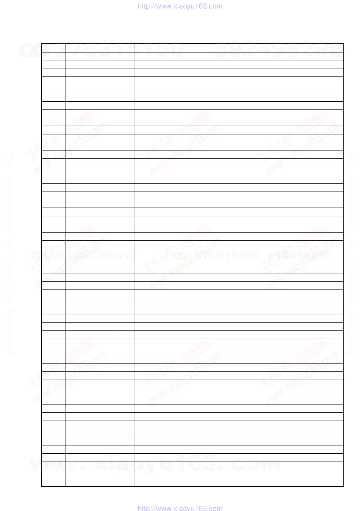
Pin No. Pin Name I/O Function
B9
B10
B11
B12
B13
B14
B15
B16
B17
B18
B19
B20
B21
B22
B23
B24
C1
C2
C3
C4
C5
C6
C7
C8
C9
C10
C11
C12
C13
C14
C15
C16
C17
C18
C19
C20
C21
C22
C23
C24
D1
D2
D3
D4
D5
D6
D7
D8
D9
D10
D11
D12
D13
DDQM3
Not open to public
Not open to public
Not open to public
Not open to public
Not open to public
Not open to public
Not open to public
Not open to public
SS0CKIN/GPIO44
DA2_VDD3
COMP1
VA C
VREF
VA G
COMP0
DCLK
DWEB
DCS0B
DADD10
DADD02
DDQS1
DQ14
DQ10
DDQS3
DILM
Not open to public
Not open to public
Not open to public
Not open to public
Not open to public
Not open to public
Not open to public
SDA1
AOBCK
AIOMCK0
DA1_VDD3
DA1_GND
VCOMB
VRTB
DADD06
DADD07
DADD08
DADD11
DCKE
DQ30
DQ28
DQ26
DQ24
PHY_D7
PHY_D5
PHY_D3
PHY_D1
O
I
O
O
O
O
O
O
I/O
—
—
—
O
I
O
—
O
O
O
O
O
I/O
I/O
I/O
I/O
—
O
O
O
O
O
O
I
I/O
O
I/O
—
—
—
—
O
O
O
O
O
I/O
I/O
I/O
I/O
I/O
I/O
I/O
I/O
Output of data mask [3]
Input of monitor sense
Output of data [11]
Output of data [8]
Output of data [5]
Output of data [2]
Output of data enable
Output of HDMI TDMS control
Input/output of DDC clock
Fixed at “L”
Power supply input (3.0V for DAC)
Fixed at “L”
Output of DA converter for video signal chrominance
Input of reference voltage
Output of DA converter for analog video signal green/Y
Fixed at “L”
Output of positive clock for DDRSDRAM
Output of command write enable
Output of DDRSDRAM chip select [0]
Output of DDRSDRAM address [10]
Output of DDRSDRAM address [2]
Input/output of data strobe [1]
Input/output of DDRSDRAM data [14]
Input/output of DDRSDRAM data [10]
Input/output of data strobe [3]
Fixed at “H”
Output of HDMI TDMS control
Output of data [9]
Output of data [6]
Output of data [4]
Output of data [1]
Output of horizontal synchronization
Input of hot plug detect
Input/output of serial data
Output of audio data clock
Input/output of audio master clock [0]
Power supply input (3.0V for DAC)
GND (for DAC)
Fixed at “L”
Fixed at “L”
Output of DDRSDRAM address [6]
Output of DDRSDRAM address [7]
Output of DDRSDRAM address [8]
Output of DDRSDRAM address [11]
Output of clock enable
Input/output of DDRSDRAM data [30]
Input/output of DDRSDRAM data [28]
Input/output of DDRSDRAM data [26]
Input/output of DDRSDRAM data [24]
Input/output of PHY-link data [7] for PHY
Input/output of PHY-link data [5] for PHY
Input/output of PHY-link data [3] for PHY
Input/output of PHY-link data [1] for PHY
w
w
w
.
x
i
a
o
y
u
1
6
3
.
c
o
m
Q
Q
3
7
6
3
1
5
1
5
0
9
9
2
8
9
4
2
9
8
T
E
L
1
3
9
4
2
2
9
6
5
1
3
9
9
2
8
9
4
2
9
8
0
5
1
5
1
3
6
7
3
Q
Q
TEL 13942296513 QQ 376315150 892498299
TEL 13942296513 QQ 376315150 892498299
http://www.xiaoyu163.com
http://www.xiaoyu163.com



 To Next Page