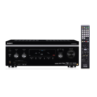
STR-DA5400ES
133
Pin No. Pin Name I/O Description
H14 DPDVBCK O
Bit clock signal output for PCM audio signal output to the lip sync adjust and D/A converter
(for audio section) (US and Canadian models)
Bit clock signal output for PCM audio signal output to the fi eld programmable gate array
(AEP, Continental European, East European, Russian and UK models)
J1, J2 AD5, AD4 I/O Two-way data bus with S-RAM and address signal output to the address latch
J4 to J6,
J9 to J11
GND - Ground terminal
J13 VDDINT - Power supply terminal (+1.2V)
J14 DPDVLRCK O
L/R sampling clock signal output for PCM audio signal output to the lip sync adjust and D/A
converter (for audio section) (US and Canadian models)
L/R sampling clock signal output for PCM audio signal output to the fi eld programmable gate
array (AEP, Continental European, East European, Russian and UK models)
K1 AD3 I/O Two-way data bus with S-RAM and address signal output to the address latch
K2 VDDINT - Power supply terminal (+1.2V)
K4 to K6,
K9 to K11,
K13
GND - Ground terminal
K14 DPSIE I PCM audio signal (surround back L/R) input from the DSP1
L1, L2 AD2, AD1 I/O Two-way data bus with S-RAM and address signal output to the address latch
L4 to L6,
L9 to L11,
L13
GND - Ground terminal
L14 DPSID I PCM audio signal (center, sub woofer) input from the DSP1
M1 AD0 I/O Two-way data bus with S-RAM and address signal output to the address latch
M2 WR O Data write enable signal output to the S-RAM
M3, M12 GND - Ground terminal
M13 DPSIB I PCM audio signal (front L/R) input from the A/D converter, HDMI receiver or DSP1
M14 DPSIC I PCM audio signal (surround L/R) input from the DSP1
N1 AD15 O Address signal output to the S-RAM and address latch
N2 ALE O Address latch enable signal output to the address latch
N3 RD O Data read enable signal output to the S-RAM
N4 VDDINT - Power supply terminal (+1.2V)
N5 VDDEXT - Power supply terminal (+3.3V)
N6 AD8 O Address signal output to the S-RAM and address latch
N7 VDDINT - Power supply terminal (+1.2V)
N8 DAI_P2 - Not used
N9 VDDEXT - Power supply terminal (+3.3V)
N10 DAI_P4 I Degital audio signal input from the DSP1
N11, N12 VDDINT - Power supply terminal (+1.2V)
N13 GND - Ground terminal
N14 DPSOE O PCM audio signal output terminal Not used
P1 to P6 AD14 to AD9 O Address signal output to the S-RAM and address latch
P7 DAI_P1 O Address signal output to the S-RAM
P8 DAI_P3 - Not used
P9 SF2_DSP2_MAS O Master/slave mode selection signal output terminal
P10 DPSOA O
PCM audio signal (front L/R) output to the lip sync adjust (US and Canadian models)
PCM audio signal (front L/R) output to the fi eld programmable gate array
(AEP, Continental European, East European, Russian and UK models)
P11 DPSOB O
PCM audio signal (surround L/R) output to the lip sync adjust (US and Canadian models)
PCM audio signal (surround L/R) output to the fi eld programmable gate array
(AEP, Continental European, East European, Russian and UK models)
P12 DPSOC O
PCM audio signal (center, sub woofer) output to the lip sync adjust
(US and Canadian models)
PCM audio signal (center, sub woofer) output to the fi eld programmable gate array
(AEP, Continental European, East European, Russian and UK models)
P13 DPSOD O
PCM audio signal (surround back L/R) output to the lip sync adjust
(US and Canadian models)
PCM audio signal (surround back L/R) output to the fi eld programmable gate array
(AEP, Continental European, East European, Russian and UK models)
P14 DPSIA I PCM audio signal (digital input) input from the DSP1
w
w
w
.
x
i
a
o
y
u
1
6
3
.
c
o
m
Q
Q
3
7
6
3
1
5
1
5
0
9
9
2
8
9
4
2
9
8
T
E
L
1
3
9
4
2
2
9
6
5
1
3
9
9
2
8
9
4
2
9
8
0
5
1
5
1
3
6
7
3
Q
Q
TEL 13942296513 QQ 376315150 892498299
TEL 13942296513 QQ 376315150 892498299
http://www.xiaoyu163.com
http://www.xiaoyu163.com