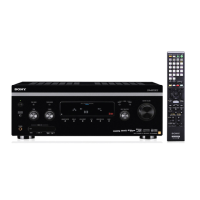
STR-DA5400ES
154
D VIDEO BOARD IC3610 MB91F467RAPMC-GE1 (VIDEO SYSTEM CONTROLLER)
Pin No. Pin Name I/O Description
1 GND - Ground terminal
2 STOP IN I AC off detection signal input terminal "L": AC off
3 DAC CLOCK SEL O Clock control signal output to the frequency multiplier for D/A converter (for video section)
4 MAIN UCOM SDA I/O Two-way I2C data bus with the system controller
5 MAIN UCOM SCL I/O Two-way I2C clock bus with the system controller
6 DAC SDA I/O Two-way I2C data bus with the D/A converter (for video section)
7 DAC SCL O I2C clock signal output to the D/A converter (for video section)
8, 9
EDID_SEL0,
EDID_SEL1
O Input data selection signal output terminal
10 NO USE - Not used
11, 12 +3.3V - Power supply terminal (+3.3V)
13 GND - Ground terminal
14 C_1 - External capacitor connection terminal for internal regulator
15 YAMAHA FLASH CE O Chip enable signal output terminal Not used
16, 17 NO USE - Not used
18 YAMAHA CE O Chip enable signal output to the OSD controller
19 SRAM CE O Chip enable signal output to the S-RAM
20 NO USE - Not used
21 YAMAHA RESET O Reset signal output to the fl ash memory and OSD controller "L": reset
22 YAMAHA WAIT_N I Wait signal input from the OSD controller
23 YAMAHA READY_N I Ready signal input terminal Not used
24 NO USE - Not used
25
SRAM OE, UB, LB/
YAMAHA RD_N
O Read enable signal output to the OSD controller and S-RAM
26 SRAM LB, WE O Lower-byte control signal and write enable signal output to the S-RAM
27
SRAM UB,WE/
YAMAHA WR_N
O
Write enable signal output to the OSD controller
Upper-byte control signal and write enable signal output to the S-RAM
28, 29 NO USE - Not used
30 TX_RST1 O Reset signal output to the HDMI transmitter "L": reset
31 TX_5VPWR1 O Power supply on/off control signal output terminal for HDMI OUT connector "H": power on
32 VDAC_RESET O Reset signal output to the D/A converter (for video section) "L": reset
33, 34 NO USE - Not used
35 RX_RST O Reset signal output to the HDMI receiver "L": reset
36 +3.3V - Power supply terminal (+3.3V)
37 C_2 - External capacitor connection terminal for internal regulator
38 GND - Ground terminal
39 X0 I Main system clock input terminal (4 MHz)
40 X1 O Main system clock output terminal (4 MHz)
41 GND - Ground terminal
42 X0A I Sub system clock input terminal Not used
43 X1A O Sub system clock output terminal Not used
44 +3.3V - Power supply terminal (+3.3V)
45 GND - Ground terminal
46 to 53
SRAM IO0 to
SRAM IO7
I/O Two-way data bus with the S-RAM
54 to 56
SRAM IO8/YAMAHA D0
to SRAM IO10/
YAMAHA D2
I/O Two-way data bus with the OSD controller and S-RAM
57 +3.3V - Power supply terminal (+3.3V)
58 GND - Ground terminal
59 to 63
SRAM IO11/YAMAHA
D3 to SRAM IO15/
YAMAHA D7
I/O Two-way data bus with the OSD controller and S-RAM
64 YAMAHA PS0 O Address signal output to the OSD controller
65, 66
SRAM A0/YAMAHA
PS1, SRAM A1/
YAMAHA PS2
O Address signal output to the OSD controller and S-RAM
w
w
w
.
x
i
a
o
y
u
1
6
3
.
c
o
m
Q
Q
3
7
6
3
1
5
1
5
0
9
9
2
8
9
4
2
9
8
T
E
L
1
3
9
4
2
2
9
6
5
1
3
9
9
2
8
9
4
2
9
8
0
5
1
5
1
3
6
7
3
Q
Q
TEL 13942296513 QQ 376315150 892498299
TEL 13942296513 QQ 376315150 892498299
http://www.xiaoyu163.com
http://www.xiaoyu163.com