4
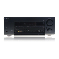
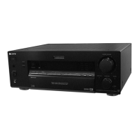
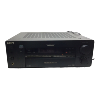
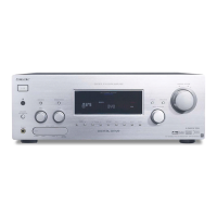
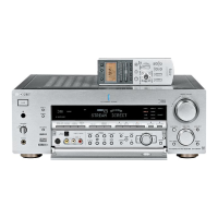
STR-DA1ES/DB780
1. SERVICING NOTES............................................... 5
2. GENERAL ................................................................... 6
3. DISASSEMBLY
3-1. Disassembly Flow ........................................................... 7
3-2. Case (414535) ................................................................. 8
3-3. S-VIDEO board, VIDEO Board and Tuner .................... 8
3-4. VIDEO.AU Board ........................................................... 9
3-5. DIGITAL Board .............................................................. 9
3-6. MAIN Board ................................................................... 10
4. TEST MODE.............................................................. 11
5. DIAGRAMS
5-1. Block Diagram
– TUNER/VIDEO INPUT Section –.............................. 13
5-2. Block Diagram – AUDIO DSP Section –...................... 14
5-3. Block Diagram – AUDIO CONTROL Section – .......... 15
5-4. Block Diagram – POWER AMP Section – ................... 16
5-5. Block Diagram
– DISPLAY/KEY CONTROL Section –........................ 17
5-6. Block Diagram – POWER SUPPLY Section – ............. 18
5-7. Note for Printed Wiring Boards
and Schematic Diagrams ................................................ 19
5-8. Schematic Diagram – DIGITAL (1/3)/
V-3 OPT Boards – ........................................................... 21
5-9. Schematic Diagram – DIGITAL Board (2/3) –............. 22
5-10. Schematic Diagram – DIGITAL Board (3/3) – ............. 23
5-11. Printed Wiring Board
– DIGITAL Board (Component Side) – ......................... 24
5-12. Printed Wiring Boards
– DIGITAL (Conductor Side)/V-3 OPT Boards – ......... 25
5-13. Printed Wiring Board – VIDEO Board –....................... 26
5-14. Schematic Diagram – VIDEO Board – ......................... 27
5-15. Printed Wiring Boards
– S-VIDEO/VIDEO 3/VIDEO.AU Boards – ................. 28
5-16. Schematic Diagram
– S-VIDEO/VIDEO 3/VIDEO.AU Boards – ................. 29
5-17. Printed Wiring Board – MAIN Board – ........................ 30
5-18. Schematic Diagram – MAIN Board (1/3) – .................. 31
5-19. Schematic Diagram – MAIN Board (2/3) – .................. 32
5-20. Schematic Diagram – MAIN Board (3/3) – .................. 33
5-21. Printed Wiring Board – BIAS Board –.......................... 34
5-22. Schematic Diagram – BIAS Board –............................. 35
5-23. Printed Wiring Boards – H.P/PRE/SPOUT Boards – ... 36
5-24. Schematic Diagram – H.P/PRE/SPOUT Boards – ....... 37
5-25. Printed Wiring Board – DISPLAY Board – .................. 38
5-26. Schematic Diagram – DISPLAY Board – ..................... 39
5-27. Printed Wiring Boards
– KEY/MUTING/POWER Boards –.............................. 40
5-28. Schematic Diagram
– KEY/MUTING/POWER Boards –.............................. 41
5-29. Printed Wiring Boards
– AC/DC 1/DC 2/PR 1/SEC 1 Boards – ......................... 42
5-30. Schematic Diagram
– AC DC 1/DC 2/PR 1/SEC 1 Boards – ......................... 43
5-31. IC Pin Function Description ........................................... 49
6. EXPLODED VIEWS
6-1. Case Section .................................................................... 55
6-2. Front Panel Section-1...................................................... 56
6-3. Front Panel Section-2...................................................... 57
6-4. Chassis Section-1 ............................................................ 58
6-5. Chassis Section-2 ............................................................ 59
6-6. Chassis Section-3 ............................................................ 60
6-7. Chassis Section-4 ............................................................ 61
6-8. BIAS Board Section........................................................ 62
6-9. MAIN Board Section ...................................................... 63
6-10. Foot Section .................................................................... 64
7. ELECTRICAL PARTS LIST ............................... 65
TABLE OF CONTENTS
 Loading...