66
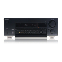
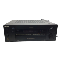
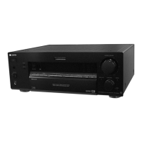
STR-DB795
Pin No.
Pin Name
I/O Description
51 NC
-
Not used
52 to 54 MD2 to MD0
-
Not used
55 RSTX
I
System reset signal input from the reset signal generator "L": reset For several hundreds msec.
after the power supply rises, "L" is input, then it changes to "H"
56 VCC
-
Power supply terminal (+3.3V)
57 X1
O
System clock output terminal (16.5 MHz)
58 X0
I
System clock input terminal (16.5 MHz)
59 VSS
-
Ground terminal
60 STOP
I
AC off detection signal input terminal
61 RDS_ CLK
I
RDS interrupt clock signal input from the tuner unit (AEP and UK models only)
62
POWER.ON/OFF
I
Power key input terminal "L": power on
63 SIRCS
I
Sircs signal input terminal
64 NC
-
Not used
65 TUNER DO
I
Serial data input from the tuner unit
66 TUNER LATCH
O
Serial data latch pulse signal output to the tuner unit
67 DIR ERROR
I
PLL lock error signal and data error flag input from the digital audio interface receiver
68 VCC
-
Power supply terminal (+3.3V)
69, 70
OPT SEL2,
OPT SEL1
O
Digital input selection signal output terminal
71 XSTATE
I
Source clock selection monitor input from the digital audio interface receiver
72 DATA0
I
Audio serial data input from the digital audio interface receiver
73 XMODE
O
System reset signal output to the digital audio interface receiver "L": reset
74 CKSEL1
O
Output clock selection signal output to the digital audio interface receiver
75 CLK
O
Clock signal output to the digital audio interface receiver
76 CE
O
Chip enable signal output to the digital audio interface receiver
77 VCC
-
Power supply terminal (+3.3V)
78 NC
-
Not used
79
DI
O
Write data output to the digital audio interface receiver
80 DO
I
Read data input from the digital audio interface receiver
81
GROUP SW
O
Data selection signal output terminal
82 LRCK SW
O
Signal selection signal output terminal "L": boot strap signal, "H": L/R sampling clock signal
83
PCM IMITATION
-
Not used
84 NC
-
Not used
85 DSP_BST
O
Boot strap signal output to the audio digital signal processor
86
CONTROL.
A1.IN
I
Sircs signal input for CONTROL A1 II
87
CONTROL.
A1.OUT
O
Sircs signal output for CONTROL A1 II
88 DSP GP9
I
Read ready signal input from the audio digital signal processor
89 DSP_HCS
O
Chip select signal output to the audio digital signal processor
90 DSP_HACN
I
Acknowledge signal input from the audio digital signal processor
91 ADC:RST
O
System reset signal output to the A/D converter "L": reset
92 DAC_RST
O
System reset signal output to the D/A converter "L": reset
93 DA1LAT
O
Serial data latch pulse signal output to the D/A converter
94 DACCLK
O
Serial data transfer clock signal output to the D/A converter
95 DAC_MDI
O
Serial data output to the D/A converter
96 DA2LAT
O
Serial data latch pulse signal output to the D/A converter