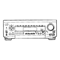
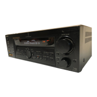
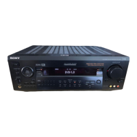
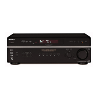
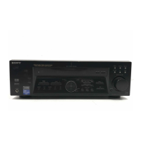
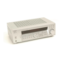
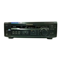
STR-DE915/TA-V909/VE910
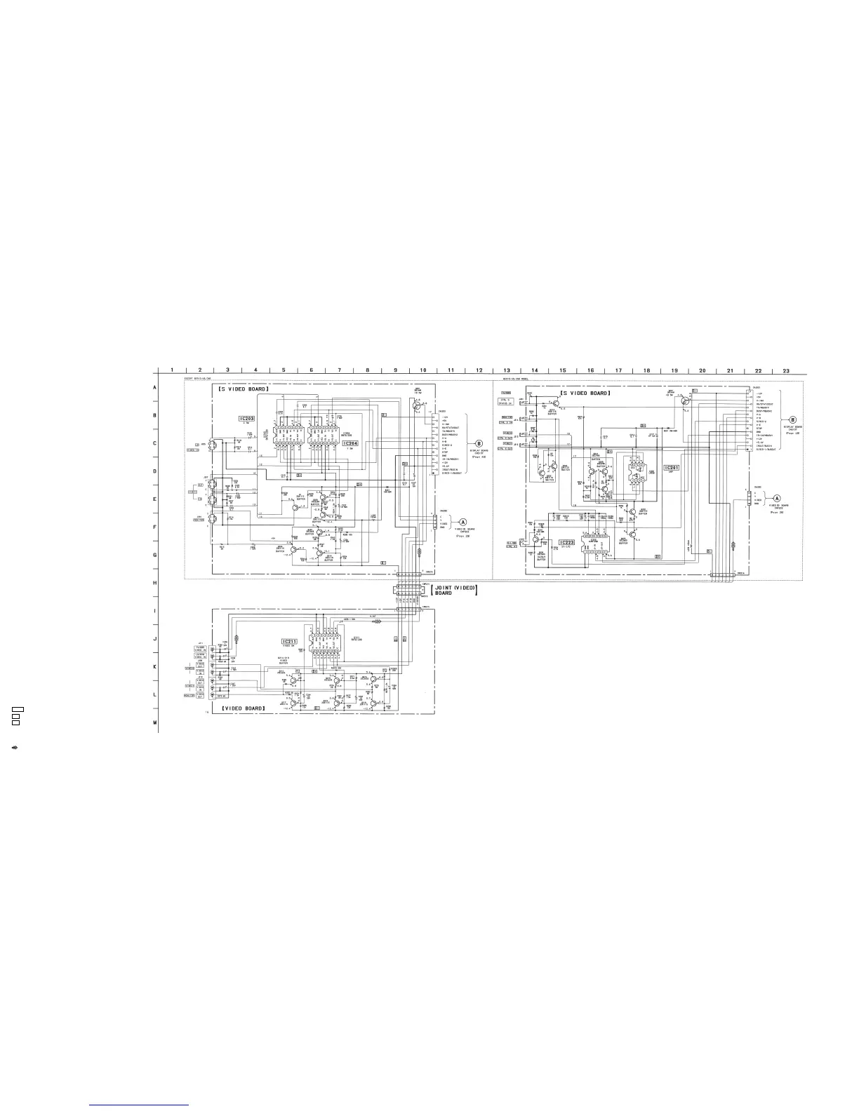
2-5. SCHEMATIC DIAGRAM — VIDEO SECTION —
Note :
• All capacitors are in µF unless otherwise noted. pF: µµF 50WV or
less are not indicated except for electrolytics and tantalums.
• All resistors are in Ω and 1/4W or less unless otherwise specified.
• : panel designation.
•
B+
: B+ Line.
•
B–
: B– Line.
• Voltage is measured with respect to ground under no-signal
conditions.
• Voltages are reference value measured by a VOM (10MΩ/V).
• Signal path
: LD (VIDEO)
• Abbreviation
CND : Canadian
— 16 — — 17 — — 18 —