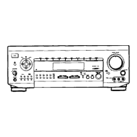
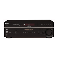
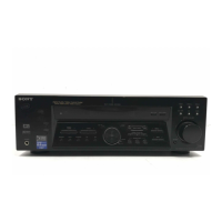
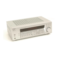
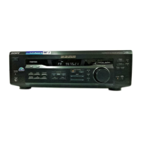
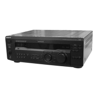
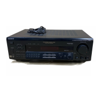
STR-DE915/TA-V909/VE910
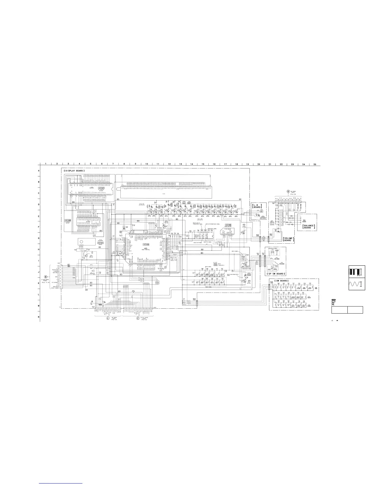
2-13. SCHEMATIC DIAGRAM — DISPLAY SECTION —
Note :
• All capacitors are in µF unless otherwise noted. pF: µµF 50WV or
less are not indicated except for electrolytics and tantalums.
• All resistors are in Ω and 1/4W or less unless otherwise specified.
• : non flammable resistor.
• : panel designation.
•
B+
: B+ Line.
•
B–
: B– Line.
• Voltage is measured with respect to ground under no-signal
conditions.
• Voltages are reference value measured by a VOM (10MΩ/V).
• Signal path
: FM : CD (ANALOG)
• Abbreviation
CND : Canadian
CH : Chinese
The components identified by
mark ! or dotted line with mark
! are critical for safety.
Replace only with part number
specified.
Les composants identifiés par
une marque ! sont critiques
pour la sécurité.
Ne les remplacer que par une
pièce portant le numéro spécifié.
— 48 — — 49 — — 50 — — 51 — — 52 —
1
IC103 @∞ FLCLK
2
IC103 ^¢ DX
4MHz
4.8Vp-p
3.5µsec
4.8Vp-p
• Waveforms