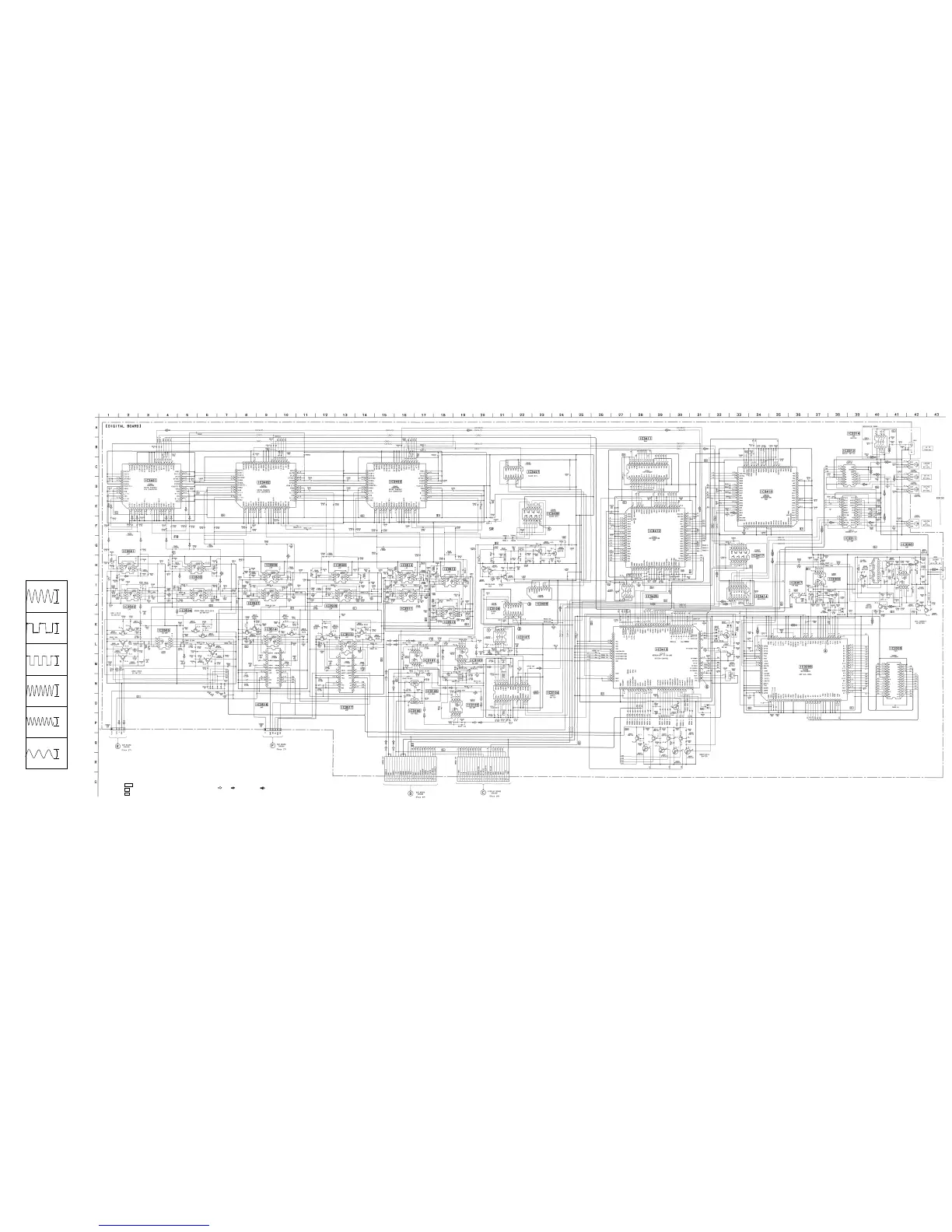
2-10. SCHEMATIC DIAGRAM — DIGITAL SECTION —
Note :
• All capacitors are in µF unless otherwise noted. pF: µµF 50WV or
less are not indicated except for electrolytics and tantalums.
• All resistors are in Ω and 1/4W or less unless otherwise specified.
• : panel designation.
•
B+
: B+ Line.
•
B–
: B– Line.
— 33 — — 34 — — 35 — — 36 — — 37—
1
IC3107 3
2
IC3108 4
3
IC3108 8
48kHz
3.072MHz
12.288MHz
4
IC3308 %§ VOUT
18.432MHz
5
IC3408 !£
6
IC3413 *™ X IN
4MHz
49.152MHz
3.5Vp-p
5.4Vp-p
4.6Vp-p
5.8Vp-p
2.2Vp-p
4.6Vp-p
• Waveforms
• Voltage is measured with respect to ground under no-signal
conditions.
• Voltages are reference value measured by a VOM (10MΩ/V).
• Signal path
: FM : CD (ANALOG) : CD (DIGITAL)