STR-DN1050
76
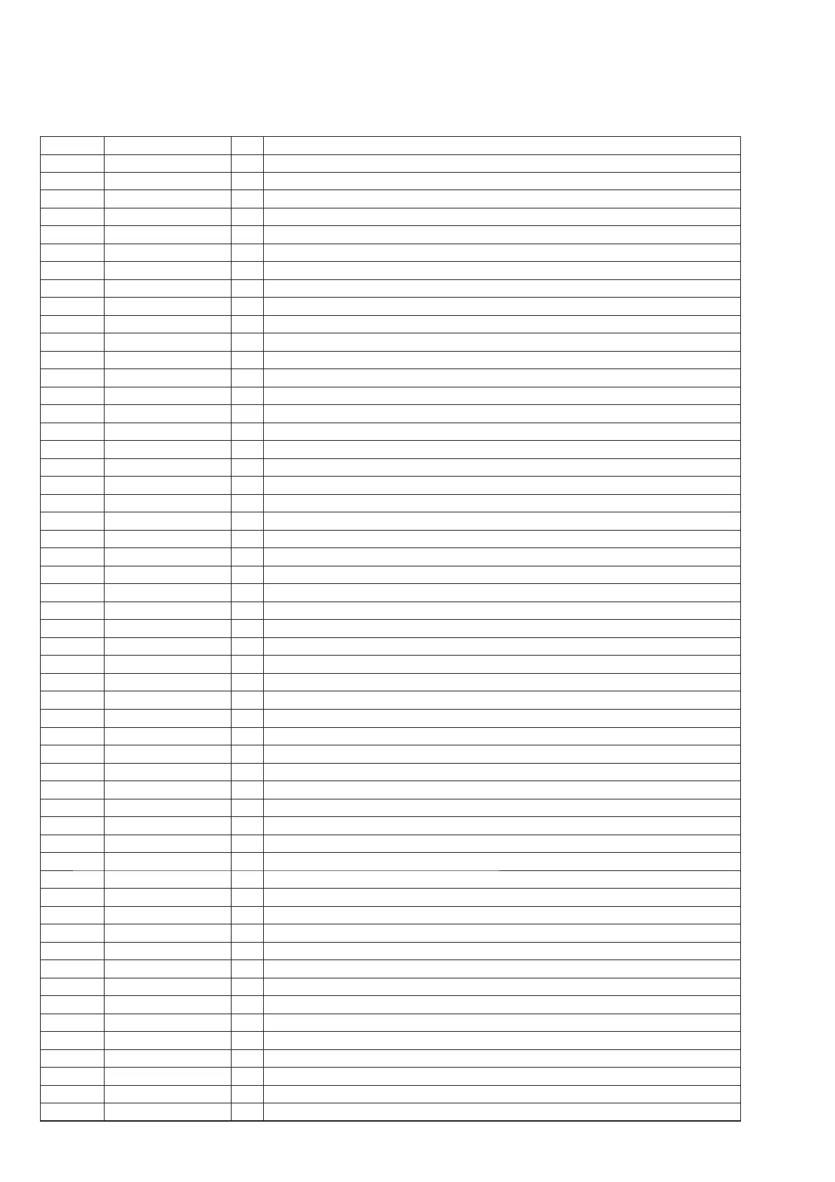
Pin No. Pin Name I/O Description
1 VCC - Power supply pin (+3.3V)
2 EVOL_CLK O I2C clock signal output to the electrical volume
3 EVOL_DATA O I2C data output to electrical volume
4 HP_DET I Headphone detection signal input
5 NC - Not connected
6 DAC_ZERO_DATA I Input signal from DAC when 0 Data
7 M0 O NW_DSD_Multiplier Select_M0
8 M1 O NW_DSD_Multiplier Select_M1
9 NC - Not connected
10 TUNER_CLK O I2C clock signal output to the tuner (FM/AM)
11 TUNER_MOSI I/O
I2C data output to the tuner (FM/AM)
12 TUN_RDS_SIGNAL I RDS data signal input (for destination that support RDS only)
13 TUNER_CE O Tuner IC enable port.
14 DIR FSRATE I Sampling rate frequency from the digital audio interface receiver
15 DAC_IIC_SCL O IIC clock output to D/A converter.
16 DAC_IIC_SCA I/O IIC data output to D/A converter.
17 DIR_INT I DIR interrupt
18 DIR_XSTATE I Clock selection signal input from the digital audio interface receiver
19 DIR_SIGNAL I Audio serial data input from the digital audio interface receiver
20 DIR_RST O Reset signal output to the digital audio interface receiver
21 DIR_CE O Chip enable signal output to the digital audio interface receiver
22 DIR_MISO I Serial data input from digital audio interface receiver
23 DIR_SPICLK O Serial clock output to digital audio interface receiver.
24 DIR_MOSI O Serial data output to digital audio interface receiver
25 VSS - Ground terminal
26 VCC - Power supply pin (+3.3V)
27 DSP_INT I Interrupt status signal input from DSP
28 DSP_SFLASH_HOLD O Hold signal output to the serial fl ash
29 DSP_RST O System reset signal output to the DSP “L” reset
30 NC - Not connected
31 DSP_NPCM I SPDIF / IIS NPCM signal input from digital audio interface receiver / HDMI receiver
32 DSP_ERROR I SPDIF / IIS Error signal input from digital audio interface receiver / HDMI receiver
33 C - Regulator stabilization capacity connecting pin
34 VSS - Ground terminal
35 VCC - Power supply pin (+3.3V)
36 HDMI_CECOUT O CEC serial data output to the HDMI connector
37 DSP_SPICS O Chip select signal output to DSP
38 INITX - Main Micom Reset port
39 DSP_MISO I Serial data input from the serial fl ash and DSP
40 DSP_MOSI O Serial data output to the serial fl ash and DSP
41 DSP_SPICLK O Serial data transfer clock signal output to the serial fl ash and DSP
42 VCOM_RESET O Video Micom Ext Reset Input Pin
43 CEC_PCONT O Control the CEC relay at HDMI out terminal.
44 VCOM_SDA (OUT) O UART data output to the video micom
45 MU UART IN I UART data input from the video micom
46 MD1 - Selection of micon operation mode (Connect to VSS)
47 MD0 - Selection of micon operation mode (Connect to VSS)
48 X0
-
Main oscillator connecting pin
49 X1 - Main oscillator connecting pin
50 VSS - Ground terminal
51 VCC - Power supply pin (+3.3V)
52 INPUT_JOG I Function encoder signal input
53 FL_LAT O Latch signal output for FL DISPLAY DRIVER IC
54 FL_DATA O Serial data output for FL DISPLAY DRIVER IC
• IC Pin Function Descriptions
DIGITAL BOARD (3/12) IC2100 MB9AF156NPMC-G-JNK1E2 (SYSTEM CONTROL)