8.10
CN10, CN11, CN19, and CN20 ARDUINO
®
Uno V3 connectors
CN10, CN11, CN19, and CN20 ARDUINO
®
Uno V3 connectors are female connectors compatible with
ARDUINO
®
Uno Revision 3 standard. Most of the shields designed for ARDUINO
®
Uno V3 fit the STM32H7B3I-
DK board.
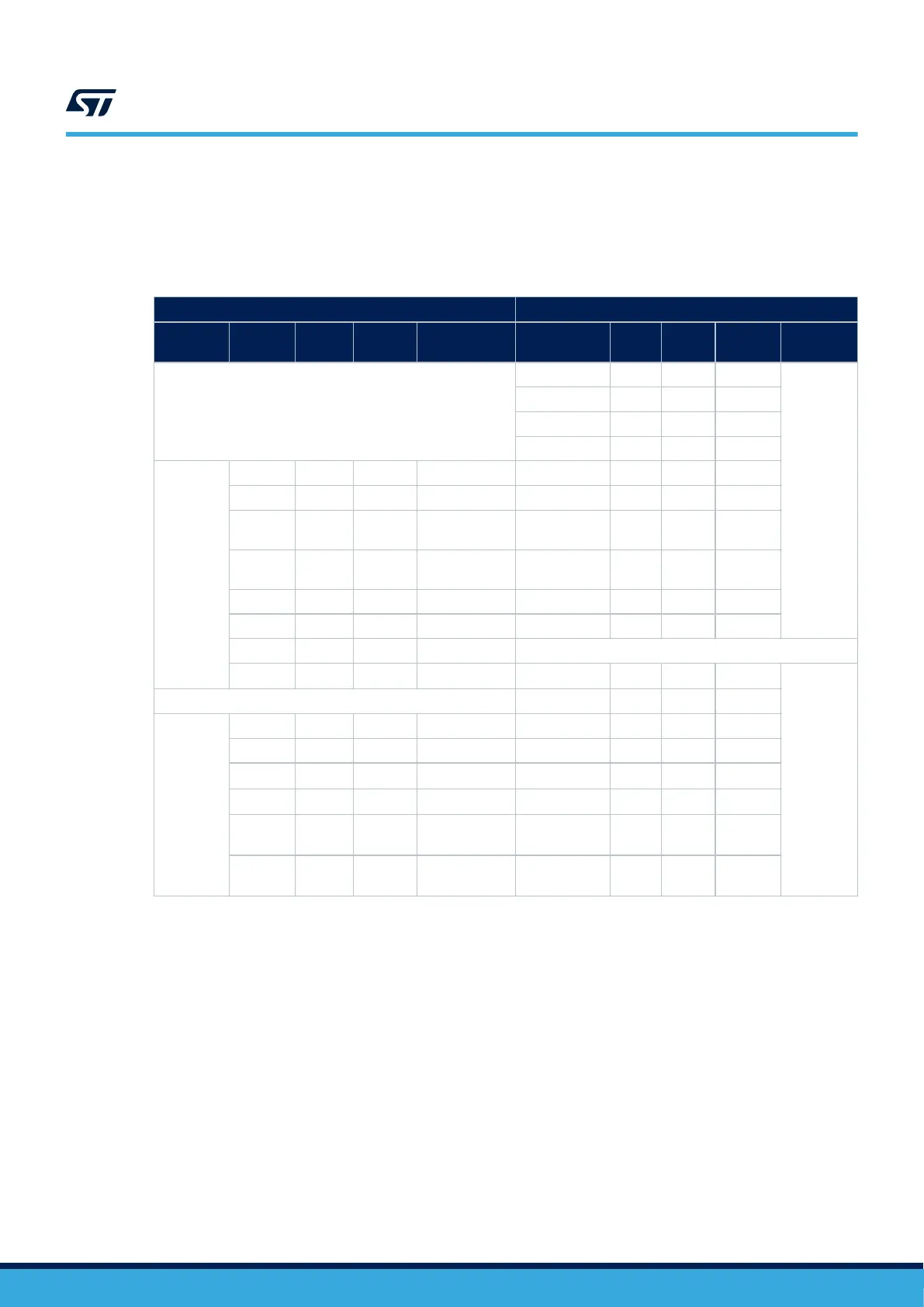
Table 23. ARDUINO
®
Uno V3 compatible connectors pinout
Left connectors Right connectors
CN
number
Pin
number
Pin
name
MCU pin Function Function
MCU
pin
Pin
name
Pin
number
CN number
-
I2C4_SCL PD12 D15 10
CN10
digital
I2C4_SDA PD13 D14 9
AVDD - AVDD 8
Ground - GND 7
CN19
power
1 - - 5V_IN test SPI2_SCK PA12 D13 6
2 IOREF - 3.3 V Ref. SPI2 _MISO PB14 D12 5
3 NRST NRST Reset
TIM1_CH3N ||
SPI2_MOSI
PB15 D11 4
4 3V3 -
3.3V output
(1)
TIM5_CH4 ||
SPI2_NSS
PI0 D10 3
5 +5V - 5 V output TIM8_CH3 PI7 D9 2
6 GND - Ground - PF10 D8 1
7 GND - Ground -
8 VIN -
Power input
(2)
- PI10 D7 8
CN11
digital
- TIM5_CH1 PH10 D6 7
CN20
analog
1 A0 PA4 ADC1_INP18 TIM5_CH2 PH11 D5 6
2 A1 PC4 ADC12_INP4 - PE2 D4 5
3
(3)
A2 PA0_C ADC1_INP0 TIM12_CH2 PH9 D3 4
4
(3)
A3 PA1_C ADC1_INP1 - PI9 D2 3
5
(3)
A4
PC2_C ||
PD13
(4)
ADC2_INP0 ||
I2C4_SDA
(4)
USART4_TX PH13 D1 2
6
(3)
A5
PC3_C ||
PD12
(4)
ADC2_INP1 ||
I2C4_SCL
(4)
USART4_RX PH14 D0 1
1. The 3V3 on ARD connector pin 4 of CN19 is not a power input for the STM32H7B3I-DK board, to simplify power
architecture.
2. The external voltage applied to pin VIN on pin 8 of CN19 must be in the range of 6 to 9V at 25°C ambient temperature. If a
higher voltage is applied on the regulator U3, it may overheat and could be damaged.
3. Supports analog input only. The current capability is limited to 1 mA when used as digital input or output.
4. By default, pins 5 and 6 of the CN20 connector are connected to ADC MCU input ports PC2_C and PC3_C respectively,
thanks to the configuration of solder bridges: SB52 and SB54 closed, SB53 and SB55 opened. In case it is necessary to
connect I
2
C interface signals on pins 5 and 6 of CN20 instead of ADC inputs, open SB52 and SB54, close SB53 and SB55.
Before using any ARDUINO
®
Uno V3 shield, it is important to refer to Section 7.2 for a correct configuration of
JPx.
Caution:
The STM32 MCU I/Os are 3.3 V compatible instead of 5 V for ARDUINO
®
Uno V3.
UM2569
CN10, CN11, CN19, and CN20 ARDUINO® Uno V3 connectors
UM2569 - Rev 6
page 33/53

 Loading...


