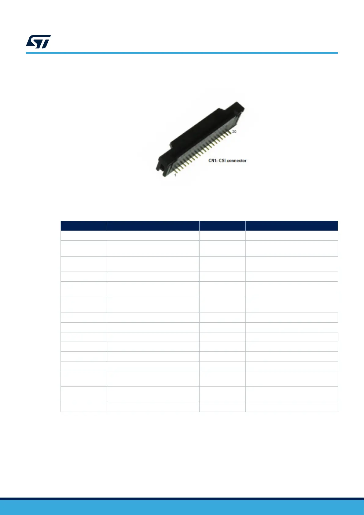
Figure 9 shows the pinout of CSI connector CN1.
Figure 9. CN1 CSI connector pinout
Table 14
describes the CSI interface and pinout of CSI connector CN1.
Table 14. CSI interface and CN1 connector pinout
Pin STM32 pin Signal name Function
1 - GND GND
2 - DATA1_N
Negative data lane 1 from MIPI-CSI
receiver 1
3 - DATA1_P
Positive data lane 1 from MIPI-CSI
receiver 1
4 - GND GND
5 - DATA2_N
Negative data lane 2 from MIPI-CSI
receiver 1
6 - DATA2_P
Positive data lane 2 from MIPI-CSI
receiver 1
7 - GND GND
8 - CKL_N Negative clock lane
9 - CKL_P Positive clock lane
10 - GND GND
11 MCP_IO3 CAM_ENABLE Camera shutdown
12 MCP_IO4 CAM_RESET Camera reset
13 PD1 I2C5_SCL
I2C5_SCL shared between USB and
touch panel
14 PH6 I2C5_SDA
I2C5_SDA shared between USB and
touch panel
15 - 3V3_SW 3V3
UM2993
CSI-DCMI
UM2993 - Rev 2
page 20/42