7 Hardware layout and configuration
7.1 Hardware layout
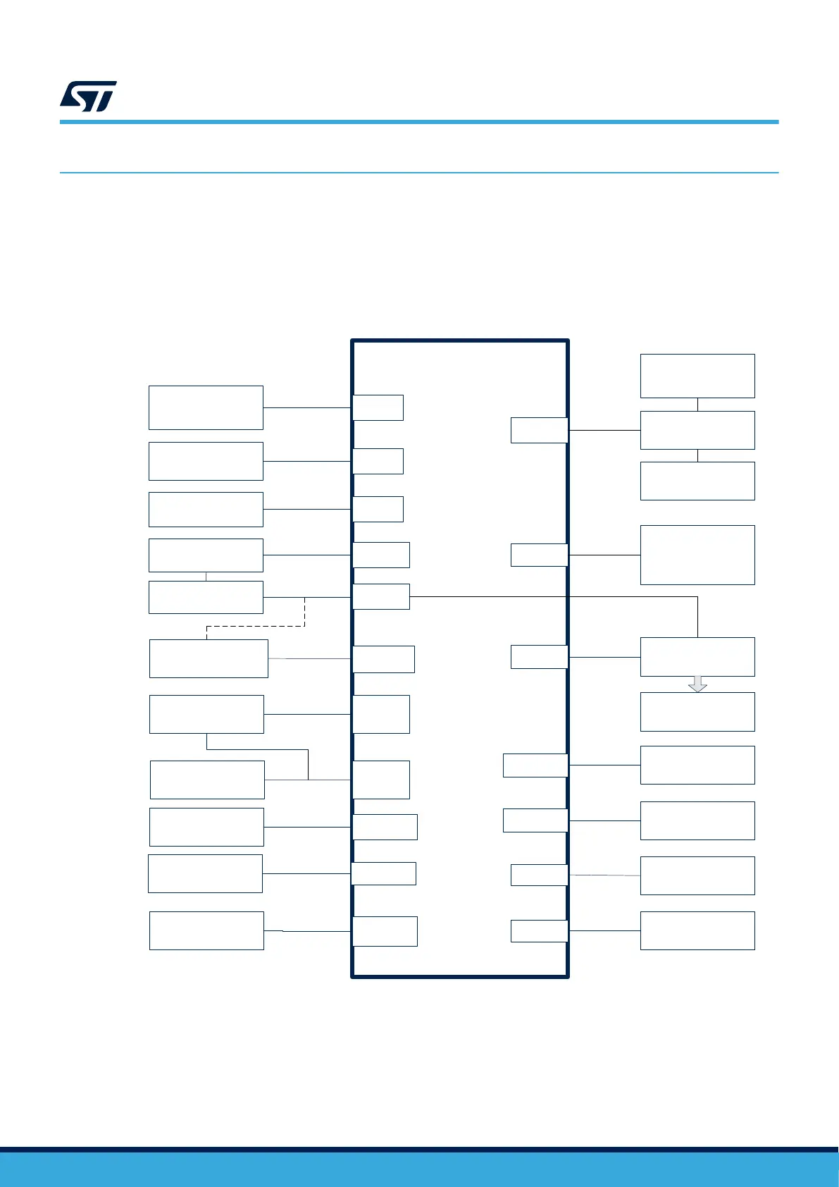
The STM32MP135F-DK is designed around the STM32MP135FAF7 microprocessor (320 pins in a TFBGA
package). The hardware block diagram (see Figure 3) illustrates the connection between the STM32MP135FAF7
microprocessor and the peripherals (such as dual Ethernet, MIPI CSI-2
®
camera module connector, USB Type-
C
®
DRP and USB Type-A connectors, GPIO expansion, and embedded ST-LINK).
Figure 3. STM32MP135F-DK hardware block diagram
DT71708V1
STM32MP135F
HSI
I2C
24 MHz crystal
4.3" TFT 480×272
Ethernet 1
RMII
USB
OTG HS
USB OTG Type-C
®
LTDC
Bluetooth
®
low
energy V4.1
UART
GPIO
Ethernet 2
RMII
DDR
I2C STPMIC1
Wake-up button
DCMI
MIPI CSI-2
®
bridge
32 kHz crystal
DDR3L
GPIO 40-pin
connector
GPIOs
STLINK-V3E
USB Micro-B
JTAG/
SWD
SDMMC
microSD™ card
connector
SDMMC
Wi-Fi
®
802.11 b/g/n
USB
HOST HS
RTC
Capacitive
touch panel
Hub: 4× USB Type-A
16-bit I/O expander
I2C
5V_VIN
USB Type-C
®
connector
2 user LEDs
2 user buttons
Tamper button
Reset button
Camera module
UM2993
Hardware layout and configuration
UM2993 - Rev 2
page 8/42