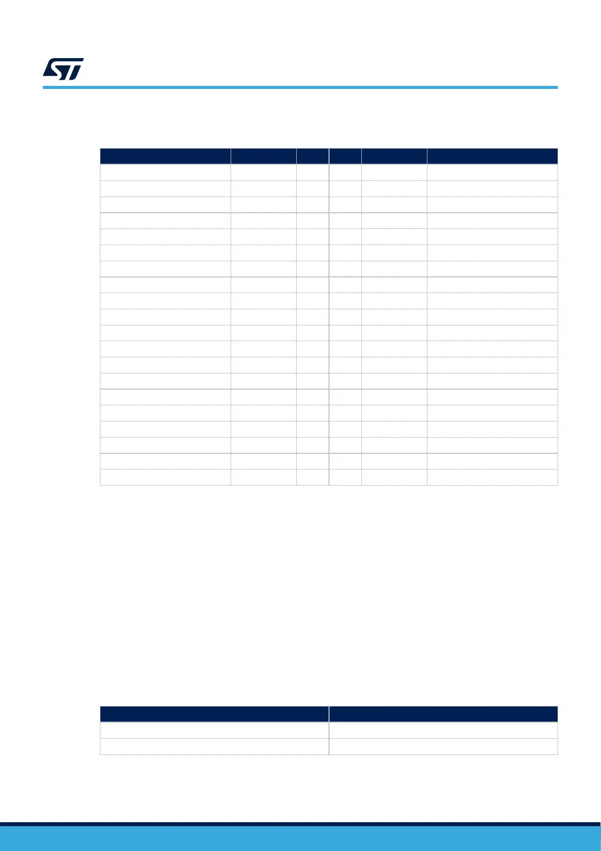
Table 18 describes the pinout of the CN8 GPIO connector.
Table 18. CN8 GPIO connector pinout
Function STM32 pin Pin Pin STM32 pin Function
3V3 - 1 2 - 5V
GPIO2 / I2C5_SDA PH6 3 4 - 5V
GPIO3 / I2C5_SCL PD1 5 6 - GND
GPIO4 / TIM3_CH4 PB1 7 8 PC0 GPIO14 / USART1_TX
GND - 9 10 PB0 GPIO15 / USART1_RX
GPIO17 / USART1_RTS PC2 11 12 PA4 GPIO18 / SAI1_SCKA
GPIO27 / DFSDM1_CKOUT PC3 13 14 - GND
GPIO22 / DFSDM1_DATIN3 PF13 15 16 PG1 GPIO23 / FDCAN2_TX
3V3 - 17 18 PG3 GPIO24 / FDCAN2_RX
GPIO10 / SPI5_MOSI PH3 19 20 - GND
GPIO9 / SPI5_MISO PA8 21 22 PI0 GPIO25 / TAMP_IN8_OUT1
GPIO11 / SPI5_SCK PH7 23 24 PH11 GPIO8 / SPI5_NSS
GND - 25 26 PF10 GPIO7
I2C1_SDA PE8 27 28 PD12 I2C1_SCL
GPIO5 / MCO2 PE6 29 30 - GND
GPIO6 / TIM4_CH2 PD13 31 32 PE5 GPIO12 / TIM8_CH3
GPIO13 /TIM14_CH1 PF9 33 34 - GND
GPIO19 / SAI1_FSA PF11 35 36 PA7 GPIO16 / USART1_CTS
GPIO26 / UART8_TX PE1 37 38 PA5 GPIO20 / SAI1_SDA
GND - 39 40 PA0 GPIO21 / SAI1_SDB
7.18 VBAT connector
7.18.1 Description
The VBAT connector allows a power mode that maintains critical operations when a power loss occurs on VDD.
The VBAT power domain contains the RTC, the backup registers, the retention RAM, and the backup SRAM. To
enable VBAT mode, a back-up power source must be connected to the VBAT connector.
7.18.2 Operating voltage
The VBAT connector allows external supply from 1.2 V to 3.6 V.
7.18.3 VBAT interface
Table 19 describes the I/O configuration of the VBAT interface.
Table 19. I/O configuration of the CN11 VBAT interface
I/O
Configuration
1 VBAT
2 GND
UM2993
VBAT connector
UM2993 - Rev 2
page 25/42