6 Hardware layout and configuration
6.1 Hardware block diagram
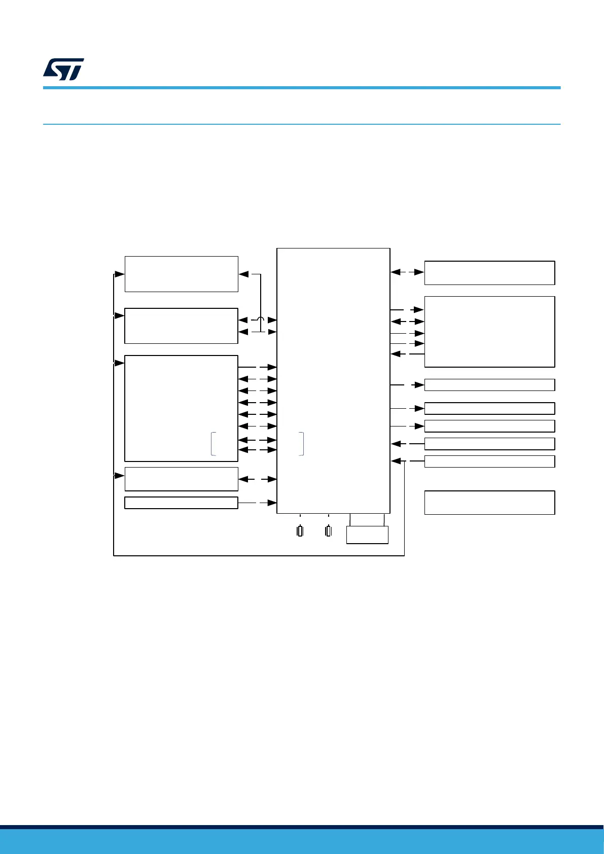
The STM32U5G9J-DK2 is designed around the STM32U5G9ZJT6Q microcontroller in an LQFP144 package. The
hardware block diagram in Figure 4 illustrates the connection between the STM32U5G9ZJT6Q microcontroller
and the peripherals. Figure 5 and Figure 6 show the locations of these features on the STM32U5G9J-DK2
Discovery board.
Figure 4. STM32U5G9J-DK2 hardware block diagram
DT59217V1
STLINK_V3EC
USB Type-C
®
Octo-SPI
16MHz
crystal
32 KHz
crystal
ARDUINO
®
Uno
V3 connector
Boot switch
User button
Reset button
Red user LED
Green user LED
5" LCD
capacitive
touch panel
(MB1860 on
RGB connector)
USB Type-C
®
connector
External debug
MIPI10 and
Tag-Connect™
SWD/JTAG
4
4
4
UART
22
Hexa-SPI
11
BOOT0
1
LCD
I2C
2
GPIO
1
RGB888 and ctrl
Touch panel
ON/OFF
Backlight
Touch-panel
interrupt
PWM
GPIO
GPIO
1
GPIO
1
GPIO
1
NRST
USB DP/DM USB DP/DM
OCTOSPI
Reset
Reset
Reset
SWD/
JTAG
UART
SWD/JTAG
Reset
ADCs
ADC/I2C
I2C
UART
ADCs
ADC/
I2C
2
4
I2C
2
PWM
UART
2
PWM
4
GPIOs GPIOs
4
PWM
SPI
PWM
1
SPI
OSC32K
2
OSC
2
Discrete
components
DC/DC
3V3 power supply
Extension connector
GPIOs
16
STM32U5G9ZJT6Q
1
1
2
3
28
1
UM3223
Hardware layout and configuration
UM3223 - Rev 1
page 7/37

 Loading...


