2-14
PDSBA-Q+/PDSBA+/PDSBA/PDSBE User's Manual
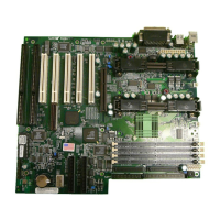
S
UPER PDSBA+
®
Processor
JPWAKE
4-PinPWR
KB/MS
USB3/4/5/6
USB1/2
LAN
Fan3
Clock
Intel
North Bridge
PCI-E x1
PCI-E x16
PCI-E x4
PCI-33MHz
LAN
CTRL
JPL1
COM2
FWH
JL1
JWOR
I-SATA0
I-SATA1
F
P CT
RL
F
a
n
2
Buzzer
2
4-Pin
ATX PWR
Supe
r IO
Fan1/CPU Fan
Intel
J44
DIMM#1A (Blue)
DIMM#2A (Black)
DIMM#1B (Blue)
DIMM#2B (Black)
Floppy
Audio
WOL
JBT1
South Bridge
J12
Battery
J
PUSB1
J
PUSB2
COM1
JF
SB1
JFSB2
Slot7
Slot6
Slot5
Slot4
JI
2
C1
JI
2
C2
PCI-33MHz
Slot3
PCI-33MHz
Slot2
Slot1
PCI-33MHz
J9
I-SATA4
I-SATA5
RAIDLED
USB7/8
J45
USB9/10
LE1
JLED
JWD
CD1
Parallel Port
VGA
HDA
IDE#2
IDE#1
ITE
J
P2
JP3
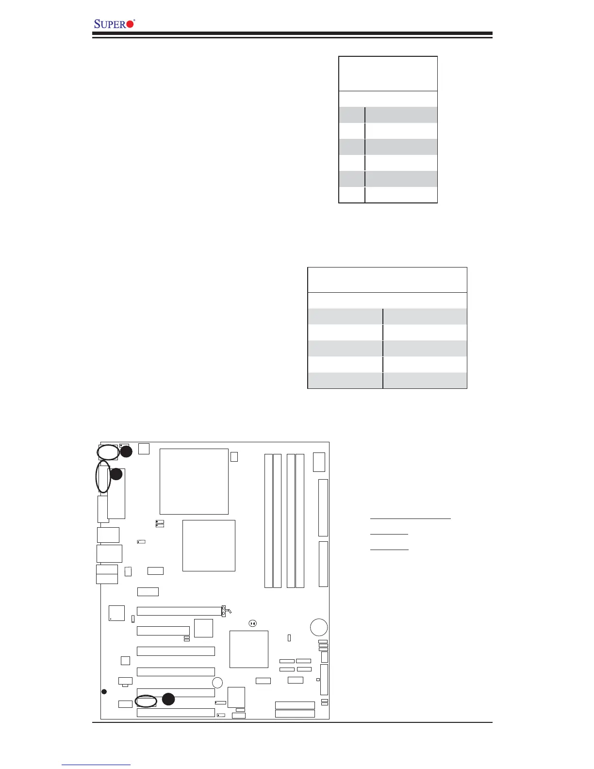
ATX PS/2 Keyboard and PS/2
Mouse Ports
The ATX PS/2 keyboard and the PS/2
mouse are located at J28. See the
table on the right for pin defi nitions.
(The mouse port is above the key-
board port.) See the table on the right
for pin defi nitions.
PS/2 Keyboard and
Mouse Port Pin
Defi nitions
Pin# Defi nition
1 Data
2NC
3 Ground
4 VCC
5Clock
6NC
Serial Ports
COM1 (J28) is a connector located
on the IO Backpane, and COM2 is a
header located at J13. See the table
on the right for pin defi nitions.
Serial Port Pin Defi nitions
(COM1/COM2)
Pin # Defi nition Pin # Defi nition
1 CD 6 DSR
2RD 7RTS
3 TD 8 CTS
4DTR 9 RI
5 Ground 10 NC
A
B
C
A. Keyboard/Mouse
B. COM1
C. COM2
(Pin 10 is available on COM2
only. NC: No Connection.)