2-24
X9DA7/X9DAE Motherboard User's Manual
JPWR1
JPI2C1
LE1
JTPM1
FAN5
FAN7
FAN6
FAN2
FAN3
FAN1
J18
JSD1
SP1
J29
JBR1
JWD1
STBY1
JPI1
JL1
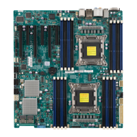
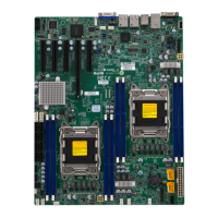
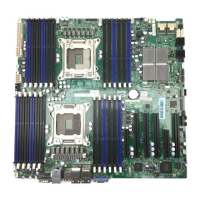
CPU1
P2 DIMMH2
P2 DIMMG2
P2 DIMMH1
P2 DIMMG1
P2 DIMME2
P2 DIMMF1
P2 DIMMF2
P1 DIMMA2
P1 DIMMA1
P1 DIMMB2
P1 DIMMB1
P1 DIMMD2
P1 DIMMD1
J25
CPU2 Slot5 PCI-E 3.0 x16
CPU1 Slot3 PCI-E 3.0 x16
CPU2 Slot2 PCI-E 3.0 x4 in x8
TPM/Port80
JF1
Always Populate DIMMxA First
CPU2
S-SATA3
I-SATA1
COM1
USB3.0 0/1
S-SATA0
P1 DIMMC2
P1 DIMMC1
JSPDIF_In
JBT1
JPME1
BIOS
JD1
LAN1/2
USB2.0
0/1/2/3
JPWR2
J22
Intel
C602
CPU2 Slot6 PCI-E 3.0 x8
J21
7.1 Audio
Audio
CTRL
GLAN
CTRL
CPLD
S I/O
JPL1
CPU2 Slot4 PCI-E 3.0 x8
Battery
USB3.0 2/3
1394a
CTRL
(CPU1Fan)
(CPU2 Fan)
JIPMB1
JSPDIF_Out
J30
JI2C1
X9DA7/E
Rev.
1.0
L-SAS0~3
Audio FP
SCU-SGPIO1
T-SGPIO1
CNF1
CNF2
L-SAS4~7
FANA
JI2C2
J23
S-SATA2
USB5/6
S-SATA1
I-SATA2
I-SATA3
I-SATA0
CTRL
SAS
CPU1 Slot1 PCI-E 3.0 x16
JOH1
JS6
JS7
DS1
JS5
JS4
FP CTRL
KB/Mouse
USB4
P2 DIMME1
FAN4
Power Button
OH/Fan Fail LED
1
NIC1 LINK LED
Reset Button
2
HDD LED
Power LED
Reset
PWR
Vcc
3.3V
NIC1 Act LED
Vcc
Ground
Ground
1920
3.3V
X
Ground
NMI
X
NIC2 Act LED
PWR Fail LED
NIC2 LINK LED
Power LED
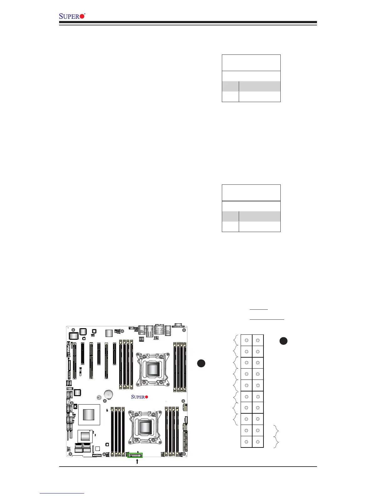
The Power LED connection is located
on pins 15 and 16 of JF1. Refer to the
table on the right for pin denitions.
NMI Button
The non-maskable interrupt button
header is located on pins 19 and 20
of JF1. Refer to the table on the right
for pin denitions.
NMI Button
Pin Denitions (JF1)
Pin# Denition
19 Control
20 Ground
Power LED
Pin Denitions (JF1)
Pin# Denition
15 3.3V
16 PWR LED
Front Control Panel Pin Denitions
A. NMI
B. PWR LED
A
B