www.ti.com
2
SNAU217A–August 2017–Revised November 2017
Submit Documentation Feedback
Copyright © 2017, Texas Instruments Incorporated
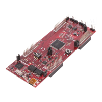
LMX2572EVM Evaluation Instructions
8 Phase Adjustment ........................................................................................................... 7
9 Calibration-Free Automatic Ramp Setting................................................................................ 8
10 Calibration-Free Automatic Ramp ......................................................................................... 8
11 Automatic Ramp Setting .................................................................................................... 9
12 Automatic Ramp ............................................................................................................. 9
13 SYSREF Pulsed Mode Setting ........................................................................................... 10
14 SYSREF Pulsed Mode .................................................................................................... 10
15 FSK SPI FAST Mode Setting............................................................................................. 11
16 FSK SPI FAST Mode ...................................................................................................... 11
17 Readback Setting .......................................................................................................... 12
18 Register Readback......................................................................................................... 12
19 LMX2572EVM Schematic (Page 1)...................................................................................... 13
20 LMX2572EVM Schematic (Page 2)...................................................................................... 14
21 PCB Layer Stack-Up....................................................................................................... 15
22 Top Layer ................................................................................................................... 15
23 GND Layer .................................................................................................................. 16
24 Power Layer ................................................................................................................ 16
25 Bottom Layer................................................................................................................ 17
26 Troubleshooting Guide .................................................................................................... 19
27 Output Termination Schematic ........................................................................................... 22
28 Default Output Phase Nosie .............................................................................................. 23
29 Default Output Waveform ................................................................................................. 23
30 Firmware Requirement .................................................................................................... 23
31 Firmware Loader ........................................................................................................... 24
32 BSL Button .................................................................................................................. 24
33 Update Firmware........................................................................................................... 25
34 Firmware Update Completed ............................................................................................. 25
35 USB Communications ..................................................................................................... 26
List of Tables
1 Loop Filter Configuration.................................................................................................... 5
2 Phase Adjustment Setting .................................................................................................. 7
3 Calibration-free Automatic Ramp Example............................................................................... 8
4 Automatic Ramp Example.................................................................................................. 9
5 FSK SPI FAST Mode Example........................................................................................... 11
6 Bill of Materials ............................................................................................................. 18
7 Reference Clock Input Configuration .................................................................................... 20
8 Reference PRO Output Frequency Selection .......................................................................... 21
9 Reference PRO Output Format Selection .............................................................................. 22
10 Output Termination Configuration........................................................................................ 22
Trademarks
All trademarks are the property of their respective owners.