Output Format Selection
www.ti.com
22
SNAU217A–August 2017–Revised November 2017
Submit Documentation Feedback
Copyright © 2017, Texas Instruments Incorporated
Reference PRO
B.2 Output Format Selection
The OE pin is used to enable or disable the output.
The OS pin is used to bias internal drivers and change the output format.
Table 9. Reference PRO Output Format Selection
OE OS OUTPUT FORMAT
GND Don't Care Disabled
Vdd GND LVPECL
Vdd NC LVDS
Vdd Vdd HCSL
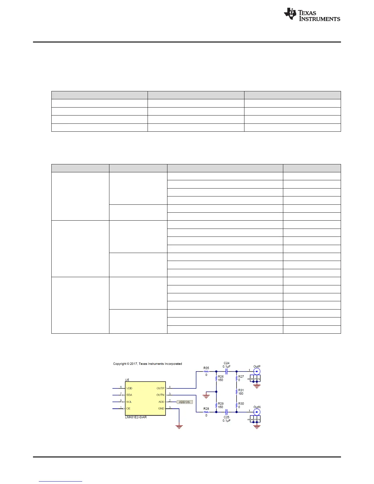
It is imperative to match the output termination passive components as shown inTable 10.
(1)
50-Ω to V
CC
– 2-V termination is required on receiver.
(2)
100-Ω differential termination (R31) is provided onboard. Removing this termination is possible if the differential termination is
available on the receiver.
Table 10. Output Termination Configuration
OUTPUT FORMAT COUPLING COMPONENT VALUE
LVPECL
AC (Default
configuration)
R15, R28 0 Ω
R26, R29 150 Ω
C24, C25 0.01 µF
R27, R30, R31 DNP
DC
(1)
R15, R28, C24, C25 0 Ω
R26, R27, R29, R30, R31 DNP
LVDS
(2)
AC
R25, R27, R28, R30 0 Ω
R31 100 Ω
C24, C25 0.01 µF
R26, R29 DNP
DC
R25, R27, R28, R30, C24, C25 0 Ω
R31 100 Ω
R26, R29 DNP
HCSL
AC
R25, R28 0 Ω
R26, R29 50 Ω
C24, C25 0.01 µF
R27, R30, R31 DNP
DC
R25, R28, C24, C25 0 Ω
R26, R29 50 Ω
R27, R30, R31 DNP
Figure 27. Output Termination Schematic