13
TMS320F28069
,
TMS320F28068
,
TMS320F28067
,
TMS320F28066
TMS320F28065, TMS320F28064, TMS320F28063, TMS320F28062
www.ti.com
SPRS698F –NOVEMBER 2010–REVISED MARCH 2016
Submit Documentation Feedback
Product Folder Links: TMS320F28069 TMS320F28068 TMS320F28067 TMS320F28066 TMS320F28065
TMS320F28064 TMS320F28063 TMS320F28062
Terminal Configuration and FunctionsCopyright © 2010–2016, Texas Instruments Incorporated
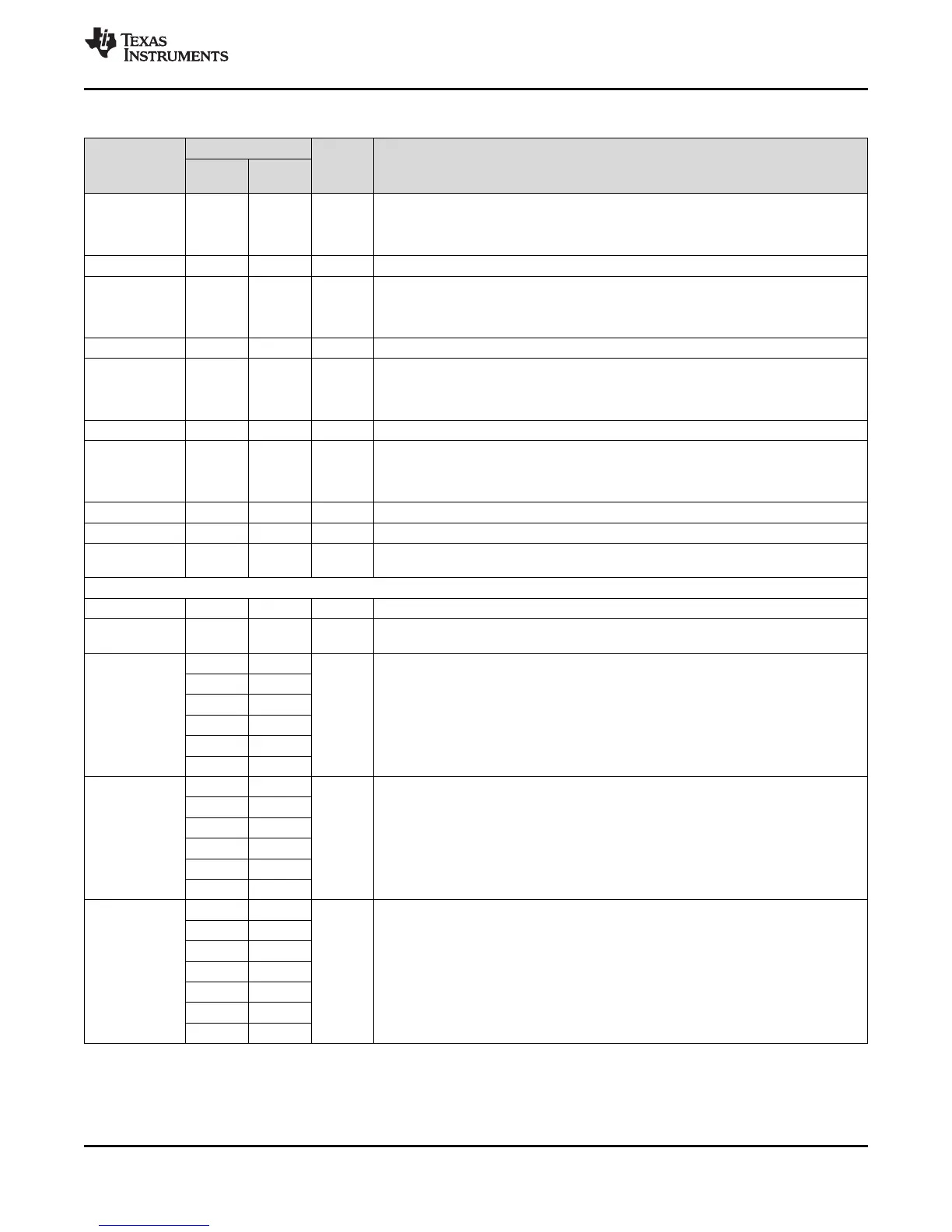
Table 4-1. Signal Descriptions
(1)
(continued)
PIN NAME
PIN NO.
I/O/Z DESCRIPTION
PZ
PZP
PN
PFP
V
REFHI
24 19
ADC External Reference High – only used when in ADC external reference mode. See
Section 6.9.2.1.
NOTE: V
REFHI
and ADCINA0 share the same pin on the 80-pin PN and PFP devices
and their use is mutually exclusive to one another.
ADCINB7 35 – I ADC Group B, Channel 7 input
ADCINB6
34 27
I ADC Group B, Channel 6 input
COMP3B I Comparator Input 3B
AIO14 I/O Digital AIO 14
ADCINB5 33 26 I ADC Group B, Channel 5 input
ADCINB4
32 25
I ADC Group B, Channel 4 input
COMP2B I Comparator Input 2B
AIO12 I/O Digital AIO12
ADCINB3 31 – I ADC Group B, Channel 3 input
ADCINB2
30 24
I ADC Group B, Channel 2 input
COMP1B I Comparator Input 1B
AIO10 I/O Digital AIO 10
ADCINB1 29 23 I ADC Group B, Channel 1 input
ADCINB0 28 22 I ADC Group B, Channel 0 input
V
REFLO
27 21
ADC External Reference Low.
NOTE: V
REFLO
is always connected to V
SSA
on the 80-pin PN and PFP devices.
CPU AND I/O POWER
V
DDA
25 20 Analog Power Pin. Tie with a 2.2-μF capacitor (typical) close to the pin.
V
SSA
26 21
Analog Ground Pin.
NOTE: V
REFLO
is always connected to V
SSA
on the 80-pin PN and PFP devices.
V
DD
3 2
CPU and Logic Digital Power Pins. When using internal VREG, place one 1.2-µF
capacitor between each V
DD
pin and ground. Higher value capacitors may be used.
14 12
37 29
63 51
81 65
91 72
V
DDIO
5 4
Digital I/O and Flash Power Pin. Single supply source when VREG is enabled. Place a
2.2-uF decoupling capacitor on each pin. The exact value of the total decoupling
capacitance should be determined by the system voltage regulation solution.
13 11
38 30
61 49
79 63
93 74
V
SS
4 3
Digital Ground Pins
15 13
36 28
47 38
62 50
80 64
92 73