17
TMS320F28069
,
TMS320F28068
,
TMS320F28067
,
TMS320F28066
TMS320F28065, TMS320F28064, TMS320F28063, TMS320F28062
www.ti.com
SPRS698F –NOVEMBER 2010–REVISED MARCH 2016
Submit Documentation Feedback
Product Folder Links: TMS320F28069 TMS320F28068 TMS320F28067 TMS320F28066 TMS320F28065
TMS320F28064 TMS320F28063 TMS320F28062
Terminal Configuration and FunctionsCopyright © 2010–2016, Texas Instruments Incorporated
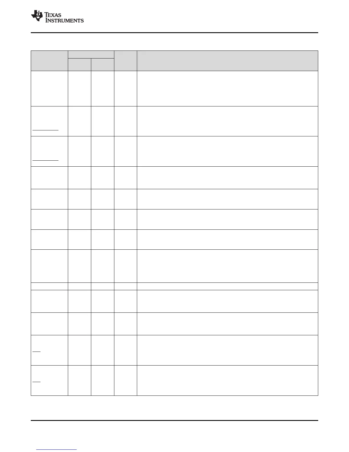
Table 4-1. Signal Descriptions
(1)
(continued)
PIN NAME
PIN NO.
I/O/Z DESCRIPTION
PZ
PZP
PN
PFP
GPIO31
40 32
I/O/Z General-purpose input/output 31
CANTXA O CAN transmit
EQEP2S I/O
Enhanced QEP2 strobe.
NOTE: eQEP2 is only available in the PZ and PZP packages.
EPWM8A O Enhanced PWM8 Output A and HRPWM channel
GPIO32
99 79
I/O/Z General-purpose input/output 32
SDAA I/OD I
2
C data open-drain bidirectional port
EPWMSYNCI I Enhanced PWM external sync pulse input
ADCSOCAO O ADC start-of-conversion A
GPIO33
100 80
I/O/Z General-purpose input/output 33
SCLA I/OD I
2
C clock open-drain bidirectional port
EPWMSYNCO O Enhanced PWM external synch pulse output
ADCSOCBO O ADC start-of-conversion B
GPIO34
68 55
I/O/Z General-purpose input/output 34
COMP2OUT O Direct output of Comparator 2
COMP3OUT O Direct output of Comparator 3
GPIO35
71 57
I/O/Z General-purpose input/output 35
TDI
I
JTAG test data input (TDI) with internal pullup. TDI is clocked into the selected register
(instruction or data) on a rising edge of TCK.
GPIO36
72 58
I/O/Z General-purpose input/output 36
TMS
I
JTAG test-mode select (TMS) with internal pullup. This serial control input is clocked
into the TAP controller on the rising edge of TCK.
GPIO37
70 56
I/O/Z General-purpose input/output 37
TDO
O/Z
JTAG scan out, test data output (TDO). The contents of the selected register
(instruction or data) are shifted out of TDO on the falling edge of TCK (8 mA drive).
GPIO38
67 54
I/O/Z General-purpose input/output 38
XCLKIN
I
External Oscillator Input. The path from this pin to the clock block is not gated by the
mux function of this pin. Care must be taken to not enable this path for clocking if it is
being used for the other functions.
TCK I JTAG test clock with internal pullup
GPIO39 66 53 I/O/Z General-purpose input/output 39
GPIO40
82 –
I/O/Z General-purpose input/output 40
EPWM7A O Enhanced PWM7 output A and HRPWM channel
SCITXDB O SCI-B transmit data
GPIO41
76 –
I/O/Z General-purpose input/output 41
EPWM7B O Enhanced PWM7 output B
SCIRXDB I SCI-B receive data
GPIO42
1 –
I/O/Z General-purpose input/output 42
EPWM8A O Enhanced PWM8 output A and HRPWM channel
TZ1 I Trip zone input 1
COMP1OUT O Direct output of Comparator 1
GPIO43
8 –
I/O/Z General-purpose input/output 43
EPWM8B O Enhanced PWM8 output B
TZ2 I Trip zone input 2
COMP2OUT O Direct output of Comparator 2