KCU105 Board User Guide www.xilinx.com 76
UG917 (v1.4) September 25, 2015
Chapter 1: KCU105 Evaluation Board Features
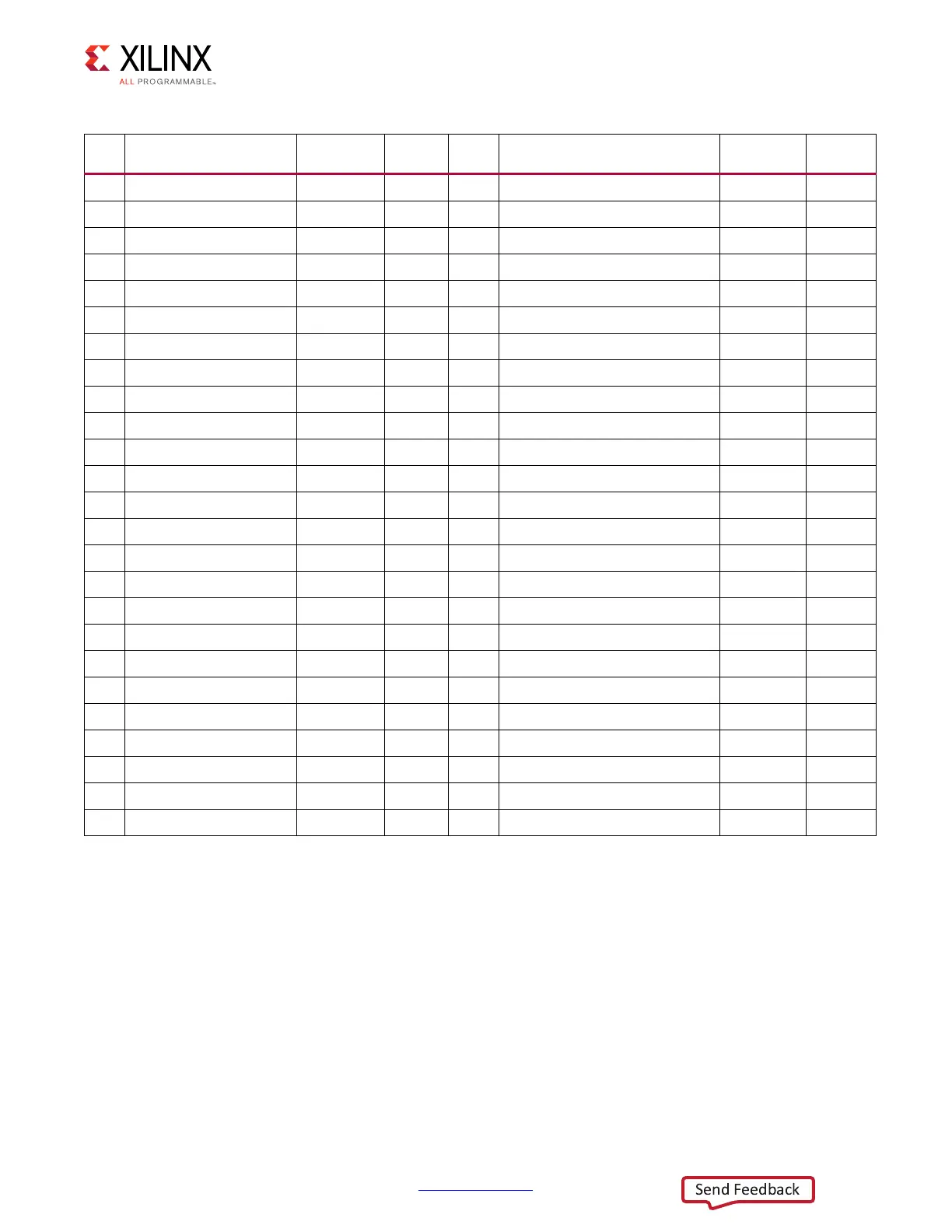
G6 FMC_LPC_LA00_CC_P LVCOMS18 W23 H4 FMC_LPC_CLK0_M2C_P LVDS AA24
G7 FMC_LPC_LA00_CC_N LVDS W24 H5 FMC_LPC_CLK0_M2C_N LVDS AA25
G9 FPC_LPC_LA03_P LVDS W28 H7 FMC_LPC_LA02_P LVDS AA22
G10 FPC_LPC_LA03_N LVDS Y28 H8 FMC_LPC_LA02_N LVDS AB22
G12 FMC_LPC_LA08_P LVDS U24 H10 FMC_LPC_LA04_P LVDS U26
G13 FMC_LPC_LA08_N LVDS U25 H11 FMC_LPC_LA04_N LVDS U27
G15 FMC_LPC_LA12_P LVDS AC22 H13 FMC_LPC_LA07_P LVDS V22
G16 FMC_LPC_LA12_N LVDS AC23 H14 FMC_LPC_LA07_N LVDS V23
G18 FMC_LPC_LA16_P LVDS AB21 H16 FMC_LPC_LA11_P LVDS V21
G19 FMC_LPC_LA16_N LVDS AC21 H17 FMC_LPC_LA11_N LVDS W21
G21 FMC_LPC_LA20_P LVDS AA34 H19 FMC_LPC_LA15_P LVDS AB25
G22 FMC_LPC_LA20_N LVDS AB34 H20 FMC_LPC_LA15_N LVDS AB26
G24 FMC_LPC_LA22_P LVDS AC34 H22 FMC_LPC_LA19_P LVDS AA29
G25 FMC_LPC_LA22_N LVDS AD34 H23 FMC_LPC_LA19_N LVDS AB29
G27 FMC_LPC_LA25_P LVDS AE33 H25 FMC_LPC_LA21_P LVDS AC33
G28 FMC_LPC_LA25_N LVDS AF34 H26 FMC_LPC_LA21_N LVDS AD33
G30 FMC_LPC_LA29_P LVDS U34 H28 FMC_LPC_LA24_P LVDS AE32
G31 FMC_LPC_LA29_N LVDS V34 H29 FMC_LPC_LA24_N LVDS AF32
G33 FMC_LPC_LA31_P LVDS V33 H31 FMC_LPC_LA28_P LVDS V31
G34 FMC_LPC_LA31_N LVDS W34 H32 FMC_LPC_LA28_N LVDS W31
G36 FMC_LPC_LA33_P LVDS W33 H34 FMC_LPC_LA30_P LVDS Y31
G37 FMC_LPC_LA33_N LVDS Y33 H35 FMC_LPC_LA030_N LVDS Y32
G39 VADJ_1V8 H37 FMC_LPC_LA32_P LVDS W30
H38 FMC_LPC_LA32_N LVDS Y30
H40 VADJ_1V8
Notes:
1. U30 MAX15301 VADJ_1V8_FPGA voltage regulator power good output signal.
2. Connected to the XCKU040 U1 LS pins J25/J24 IIC_MAIN_SDA/SCL via I2C MUX U80 and level-shifter U77.
3. XCKU040 U1 JTAG TCK, TMS, TDO pins AC9, W9, U9 buffered by U19 SN74AVC8T245.
4. J2 LPC TDO-TDI connections to U27 LPC FMC JTAG bypass switch (N.C. normally closes/bypassing J2 until an FMC card
is plugged into J2).
5. J2 LPC FMC connector TDO is level-shifted by U55, and then connected to system controller U111 pin P9 and Digilent
USB JTAG module U115 TDO pin 8 in parallel.
6. FMC_LPC_PRSNT_M2C_B is the LPC FMC JTAG bypass switch U27.4 OE control signal and is also connected to the
XCKU040 U1 pin J26 via level-shifter U44.
Table 1-24: FMC LPC J2 Connections to XCKU040 Device U1 (Cont’d)
J2 Pin Schematic Net Name
I/O Standard XCKU040
(U1) Pin
J2 Pin Schematic Net Name I/O Standard
XCKU040
(U1) Pin