20 www.xilinx.com SP605 Hardware User Guide
UG526 (v1.9) February 14, 2019
Chapter 1: SP605 Evaluation Board
See the Winbond Serial Flash Memory Data Sheet for more information. [Ref 16]
See the XPS Serial Peripheral Interface Data Sheet (DS570) for more information. [Ref 4]
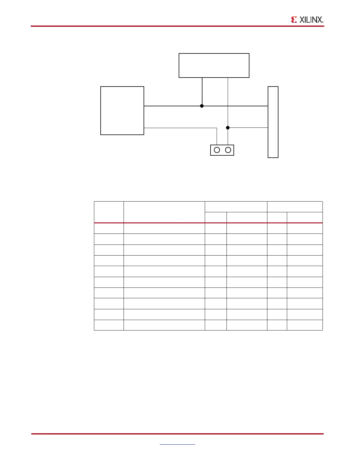
X-Ref Target - Figure 1-4
Figure 1-4: SPI Flash Interface Topology
Table 1-6: SPI x4 Memory Connections
U1 FPGA
Pin
Schematic Net Name
SPI MEM U32 SPI HDR J17
Pin # Pin Name Pin # Pin Name
AB2 FPGA_PROG_B – – 1 –
T14 FPGA_D2_MISO3 1 IO3_HOLD_B 2 –
R13 FPGA_D1_MISO2_R 9 IO2_WP_B 3 –
AA3 SPI_CS_B – – 4 TMS
AB20 FPGA_MOSI_CSI_B_MISO0 15 DIN 5 TDI
AA20 FPGA_D0_DIN_MISO_MISO1 8 IO1_DOUT 6 TDO
Y20 FPGA_CCLK 16 CLK 7 TCK
– – – –8GND
– – – – 9 VCC3V3
J46.2
(1)
SPIX4_CS_B 7 CS_B – –
Notes:
1. Not a U1 FPGA pin
U1
FPGA SPI Interface
U32
J17
SPI x4
Flash
Memory
Winbond
W25Q64FVSFIG
SPI Program
Header
SPI Select
Jumper
ON = SPI X4 U32
OFF = SPI EXT. J17
SPIX4_CS_B
DIN, DOUT, CCLK
SPI_CS_B
2
J46
1
UG526_04_020819