VC707 Evaluation Board www.xilinx.com 9
UG885 (v1.4) May 12, 2014
Overview
• Linear BPI Flash memory
• USB JTAG configuration port
• Platform cable header JTAG configuration port
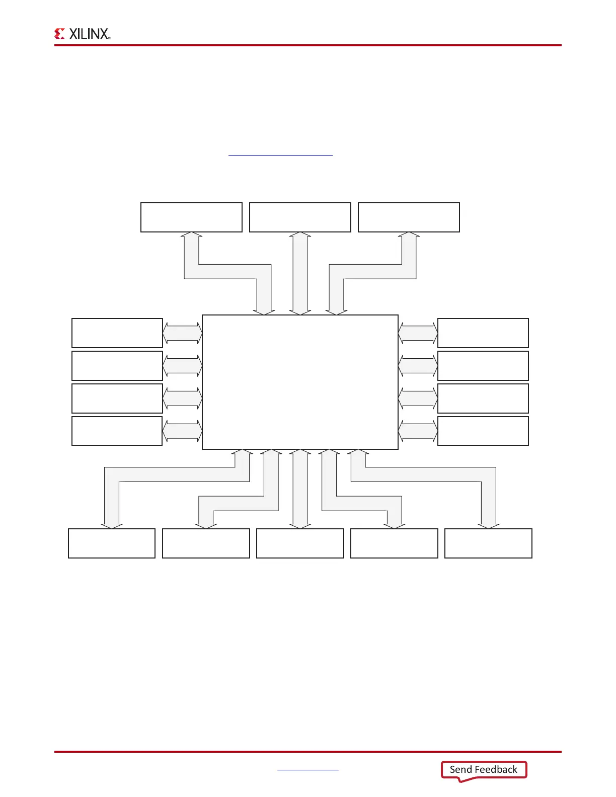
The VC707 board block diagram is shown in Figure 1-1. The VC707 board schematics are
available for download from the VC707 Evaluation Kit product page on the Docs &
Designs tab at w
ww.xilinx.com/vc707.
Caution!
The VC707 board can be damaged by electrostatic discharge (ESD). Follow
standard ESD prevention measures when handling the board.
X-Ref Target - Figure 1-1
Figure 1-1: VC707 Board Block Diagram
UG885_c1_01_030512
Virtex-7 FPGA
XC7VX485T-2FFG1761C
128 MB Linear BPI
Flash memory
USB 2.0
ULPI PHY
8-lane PCI Express
Edge Connector
LCD Display
(2 line x 16 characters)
1 KB EEPROM (I
2
C)
I
2
C Bus Switch
XADC Header
User Switches,
Buttons, and LEDs
HDMI Video
Interface
Differential Clock
GTX SMA Clock
1 GB DDR3 Memory
(SODIMM)
FMC Connectors
(HPC/HPC)
10/100/1000 Ethernet
Interface
DIP Switch SW11
Config and Flash Addr
USB-to-UART Bridge
JTAG Interface
mini-B USB Connector
SFP+ Single Cage