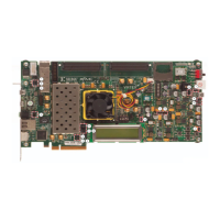
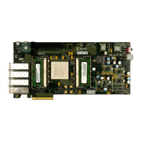
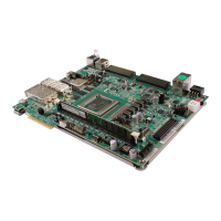
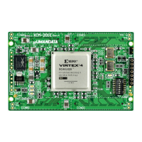
• 144 Mb 36-bit dual-port QDR-IV component memory interface (1 x [4M x 36])
• 288 MB 72-bit RLD3 component memory interface (2 x [1.125 Gb x 36])
• 2 Gb Quad SPI ash conguraon memory
• QSFPF28 - Sixteen (16) GTY transceivers are allocated for a 1x4 QSFP cage
• USB JTAG interface (FTDI FT4232HL with a micro-AB USB connector)
• Clock sources:
○ SMA I/F clocks:
- FPGA bank 67 SMA clock P/N
○ QSFP clocks:
- Four Si570 I2C programmable clock oscillators (156.25 MHz default)
- QSFP clock recovery Si5328 input to GTY132 and GTY134
- QSFP external SMA di. clock input to GTY131
○ Memory I/F clocks:
- Three SiT9120A xed 100 MHz LVDS clock oscillators
○ PCIe
®
I/F clock:
- Fixed 100 MHz HCSL clock from PCI Express
®
edge input to 1-to-2 clock buer wired
to GTY225 and GTY227
○ System controller clock:
- SiT8008A 33.33 MHz single-ended clock oscillator
• 96 GTY transceivers (24 Quads)
○ FMCP HSPC connector (twenty-four GTY transceivers)
○ 4x28 Gb/s QSFP+ connectors (eight GTY transceivers)
○ PCIe 16-lane edge connector (sixteen GTY transceivers)
○ Not used (forty-eight GTY transceivers)
• PCI Express
®
Endpoint connecvity
○ Gen1 (x1, x2, x4, x8, x16)
○ Gen2 (x1, x2, x4, x8, x16)
○ Gen3 (x1, x2, x4, x8, x16)
○ Dual Gen4 (x1, x2, x4, x8)
• Ethernet PHY SGMII interface with RJ-45 connector
• Dual USB-to-UART bridge with micro-B USB connector (shared FTDI FT4232HL)
Chapter 1: Introduction
UG1302 (v1.0) December 21, 2018 www.xilinx.com
VCU128 Board User Guide 7
 Loading...

