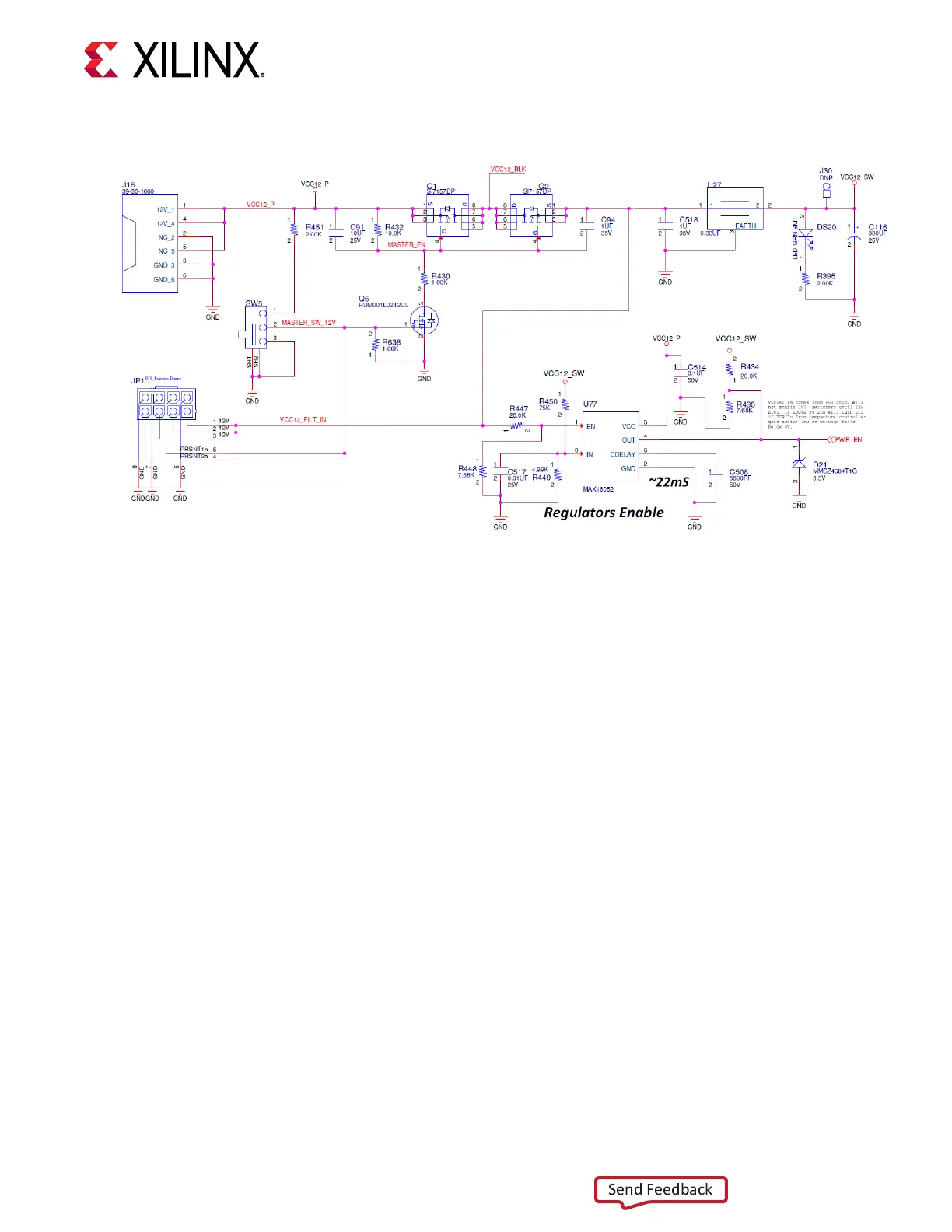
Figure 27: Power On/Off Switch SW5
X21973-112818
When the VCU128 board is used inside a computer chassis (i.e., plugged in to a PCIe
®
slot),
power is normally provided from the PC ATX supply 2x4 PCIe power connector. See Installing
the Board in a PC Chassis.
Program_B Pushbutton Switch
[Figure 2, callout 30]
Switch SW2 grounds the XCVU37P FPGA U1 PROGRAM_B pin when pressed. This acon clears
the FPGA conguraon. The FPGA_PROG_B signal is connected to XCVU37P FPGA U1 pin
BB15. See the UltraScale Architecture Conguraon User Guide (UG570) for further conguraon
details. The following gure shows SW2.
Chapter 3: Board Component Descriptions
UG1302 (v1.0) December 21, 2018 www.xilinx.com
VCU128 Board User Guide 78