VC7222 IBERT Getting Started Guide www.xilinx.com 9
UG971 (v5.0) June 12, 2014
Running the GTH IBERT Demonstration
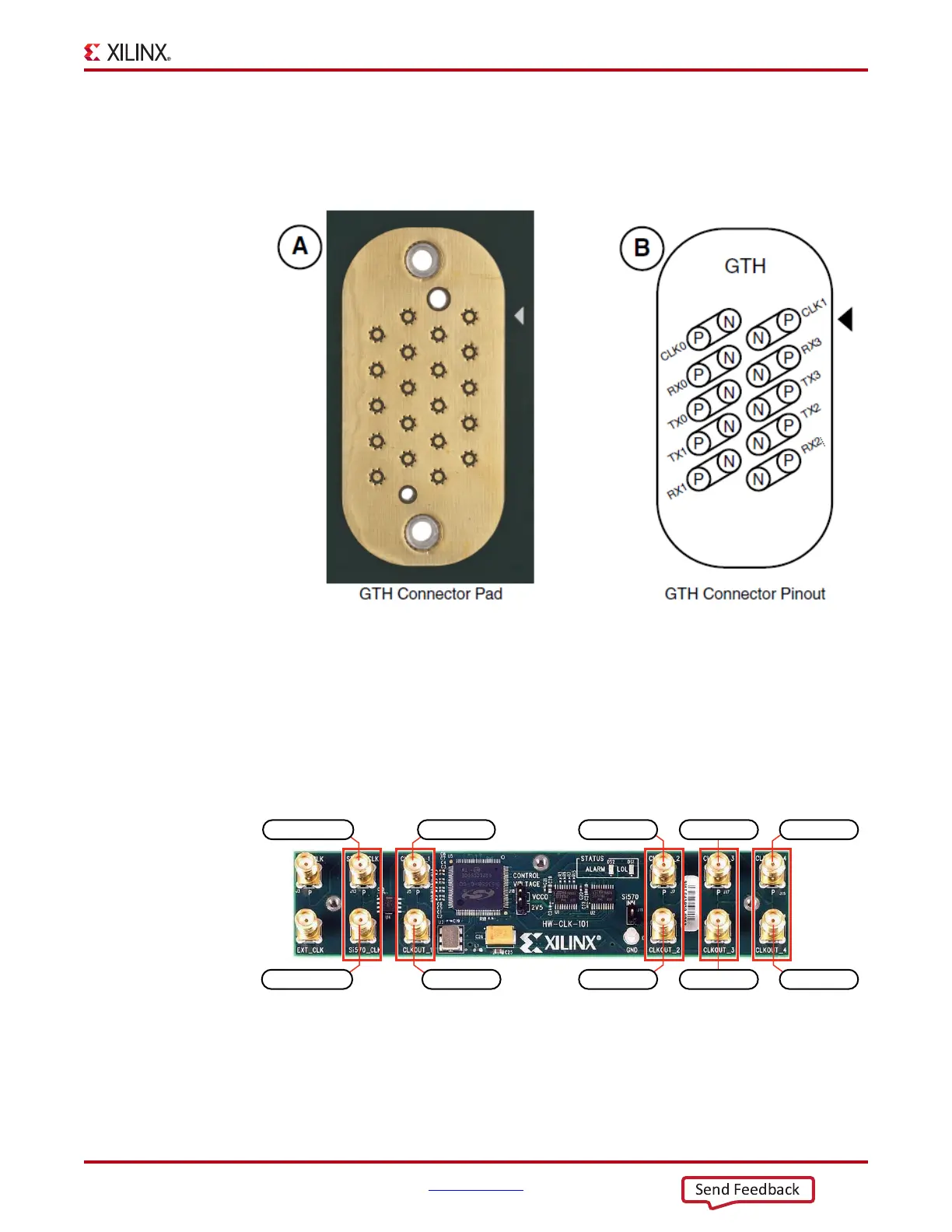
All GTH transceiver pins and reference clock pins are routed from the FPGA to a connector
pad which interfaces with the Samtec BullsEye connectors. Figure 1-2 A shows the
connector pad, and Figure 1-2 B shows the connector pinout.
The SuperClock-2 module provides LVDS clock outputs for the GTH transceiver reference
clock in the IBERT demonstration. Figure 1-3 shows the location of the differential clock
SMA connections on the clock module which can be connected to the reference clock
cables.
Note:
The image in Figure 1-3 is for reference only and might not reflect the current revision of the
board.
X-Ref Target - Figure 1-2
Figure 1-2: A – GTH Connector Pad. B – GTH Connector Pinout
X-Ref Target - Figure 1-3
Figure 1-3: SuperClock-2 Module Output Clock SMA Locations
8*BFBB
&/.287B1
&/.287B1
6,B&/.B1
6,B&/.B3
&/.287B3
&/.287B1 &/.287B1
&/.287B3 &/.287B3 &/.287B3

 Loading...


