VC7203 GTX Transceiver Characterization Board www.xilinx.com 35
UG957 (v1.3) October 17, 2014
Detailed Description
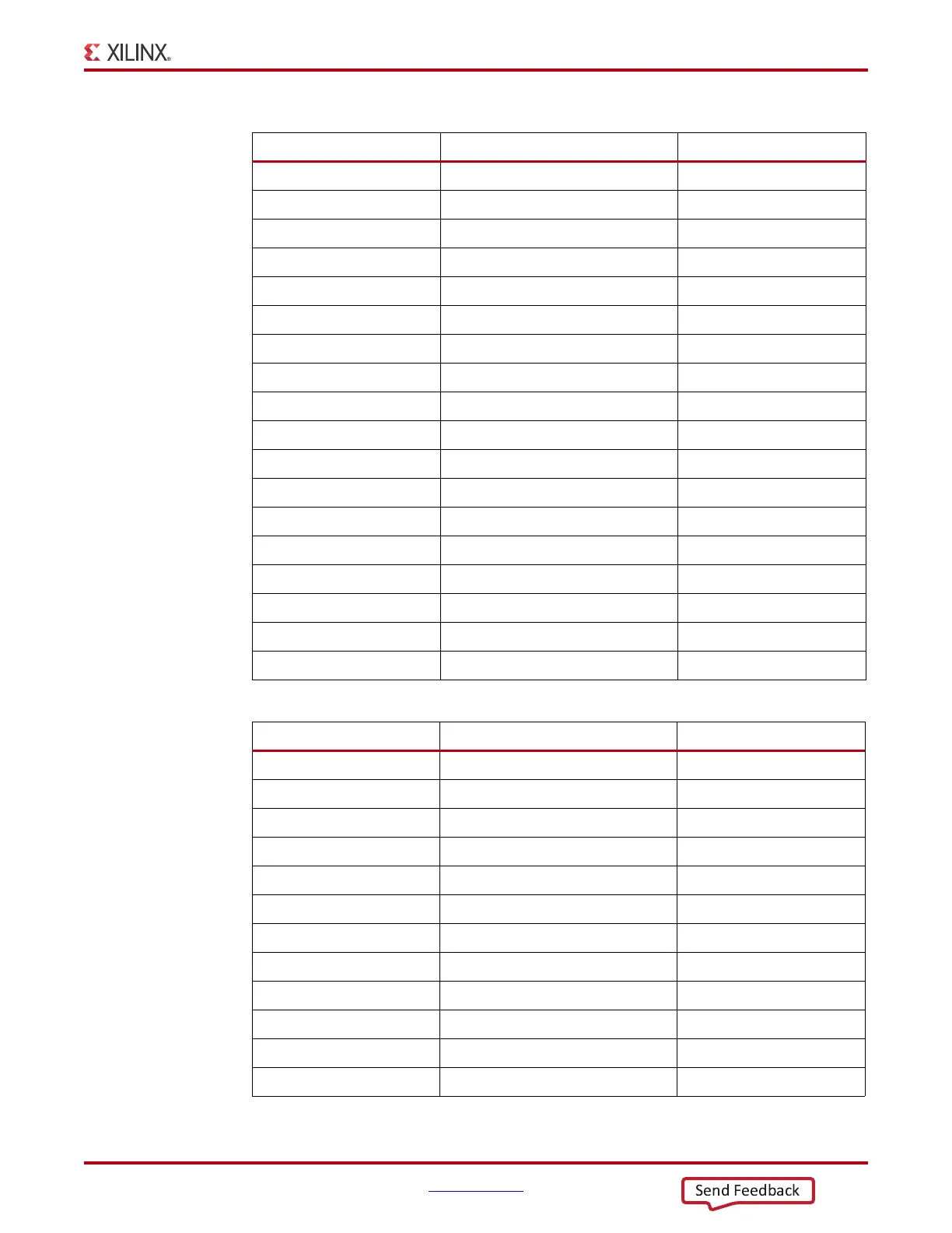
AH33 FMC1_LA25_N G28
AK35 FMC1_LA26_P D26
AL35 FMC1_LA26_N D27
AH31 FMC1_LA27_P C26
AJ31 FMC1_LA27_N C27
AH34 FMC1_LA28_P H31
AJ35 FMC1_LA28_N H32
AM34 FMC1_LA29_P G30
AN34 FMC1_LA29_N G31
AM31 FMC1_LA30_P H34
AM32 FMC1_LA30_N H35
AM33 FMC1_LA31_P G33
AN33 FMC1_LA31_N G34
AL29 FMC1_LA32_P H37
AL30 FMC1_LA32_N H38
AH29 FMC1_LA33_P G36
AH30 FMC1_LA33_N G37
AM38 FMC1_PRSNT_M2C_L H2
Table 1-19: VITA 57.1 FMC1 HPC Connections at JA3
U1 FPGA Pin Net Name FMC Pin
E34 FMC2_CLK0_M2C_P H4
E35 FMC2_CLK0_M2C_N H5
D37 FMC2_CLK1_M2C_P G2
D38 FMC2_CLK1_M2C_N G3
M24 FMC2_CLK2_BIDIR_P K4
L24 FMC2_CLK2_BIDIR_N K5
K23 FMC2_CLK3_BIDIR_P J2
J23 FMC2_CLK3_BIDIR_N J3
N30 FMC2_HA00_CC_P F4
M31 FMC2_HA00_CC_N F5
P30 FMC2_HA01_CC_P E2
N31 FMC2_HA01_CC_N E3
Table 1-18: VITA 57.1 FMC1 HPC Connections at JA2 (Cont’d)
U1 FPGA Pin Net Name FMC Pin
 Loading...
