ZCU111 Board User Guide 102
UG1271 (v1.1) August 6, 2018 www.xilinx.com
Appendix D: HW-FMC-XM500
228
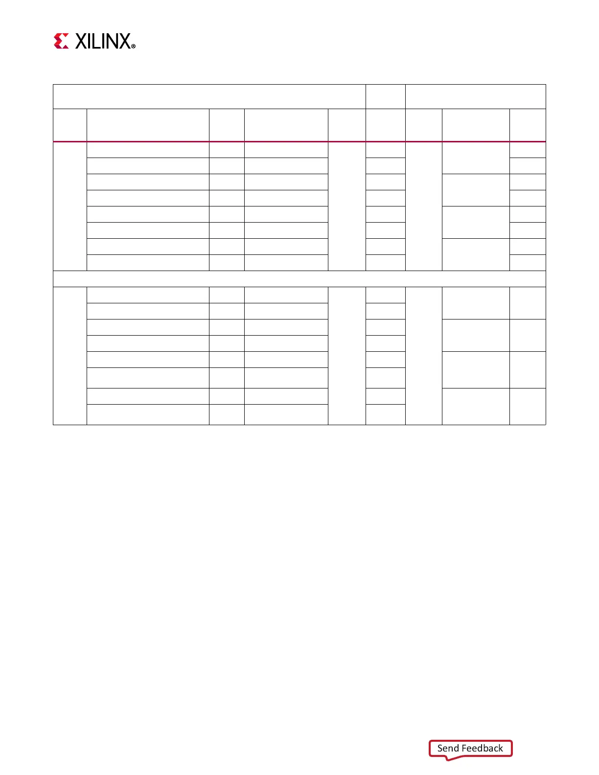
DAC_VOUT0_P_228_U2 U2 RFMC_DAC_00_P
J94
C10
J888
None, Direct
J26
DAC_VOUT0_N_228_U1 U1 RFMC_DAC_00_N B10 J27
DAC_VOUT1_P_228_R2 R2 RFMC_DAC_01_P G11
None, Direct
J20
DAC_VOUT1_N_228_R1 R1 RFMC_DAC_01_N F11 J21
DAC_VOUT2_P_228_N2 N2 RFMC_DAC_02_P C13
None, Direct
J22
DAC_VOUT2_N_228_N1 N1 RFMC_DAC_02_N B13 J23
DAC_VOUT3_P_228_L2 L2 RFMC_DAC_03_P G14
None, Direct
J24
DAC_VOUT3_N_228_L1 L1 RFMC_DAC_03_N F14 J25
229
DAC_VOUT0_P_229_J2 J2 RFMC_DAC_04_P
J94
C16
J888
U3 Anaren
Balun 1-4 GHz
J7
DAC_VOUT0_N_229_J1 J1 RFMC_DAC_04_N B16
DAC_VOUT1_P_229_G2 G2 RFMC_DAC_05_P G17
U1 Anaren
Balun 1-4 GHz
J8
DAC_VOUT1_N_229_G1 G1 RFMC_DAC_05_N F17
DAC_VOUT2_P_229_E2 E2 RFMC_DAC_06_P C19 U5
Mini-Circuits
Xfmr 0-1 GHz
J5
DAC_VOUT2_N_229_E1 E1 RFMC_DAC_06_N B19
DAC_VOUT3_P_229_C2 C2 RFMC_DAC_07_P G20 U4
Mini-Circuits
Xfmr 0-1 GHz
J6
DAC_VOUT3_N_229_C1 C1 RFMC_DAC_07_N F20
Table D-3: ZCU111 U1 RFSoC RF Bank 224-229 Connections to XM500 (Cont’d)
ZCU111 Board (with LPAF)
Mated
Conns
XM500 RFMC Card (with LPAM)
ZU28DR
U1 Bank
ZU28DR U1 Pin Name
ZU28DR
U1 Pin
ZCU111 Net Name
ZCU111
LPAF
LPAF/
M Pin
XM500
LPAM
SE-to-Diff
Element
XM500
SMA Ref
Des
 Loading...


