ZCU111 Board User Guide 37
UG1271 (v1.1) August 6, 2018 www.xilinx.com
Chapter 3: Board Component Descriptions
PMU GPO (MIO 32-37)
The platform management unit (PMU) in the Zynq UltraScale+ RFSoC device signals power
domain changes using the PMU output pins. The Zynq UltraScale+ RFSoC device PMU GPO
pins are connected to inputs of the MSP430 system controller via TXS0108E level-shifter
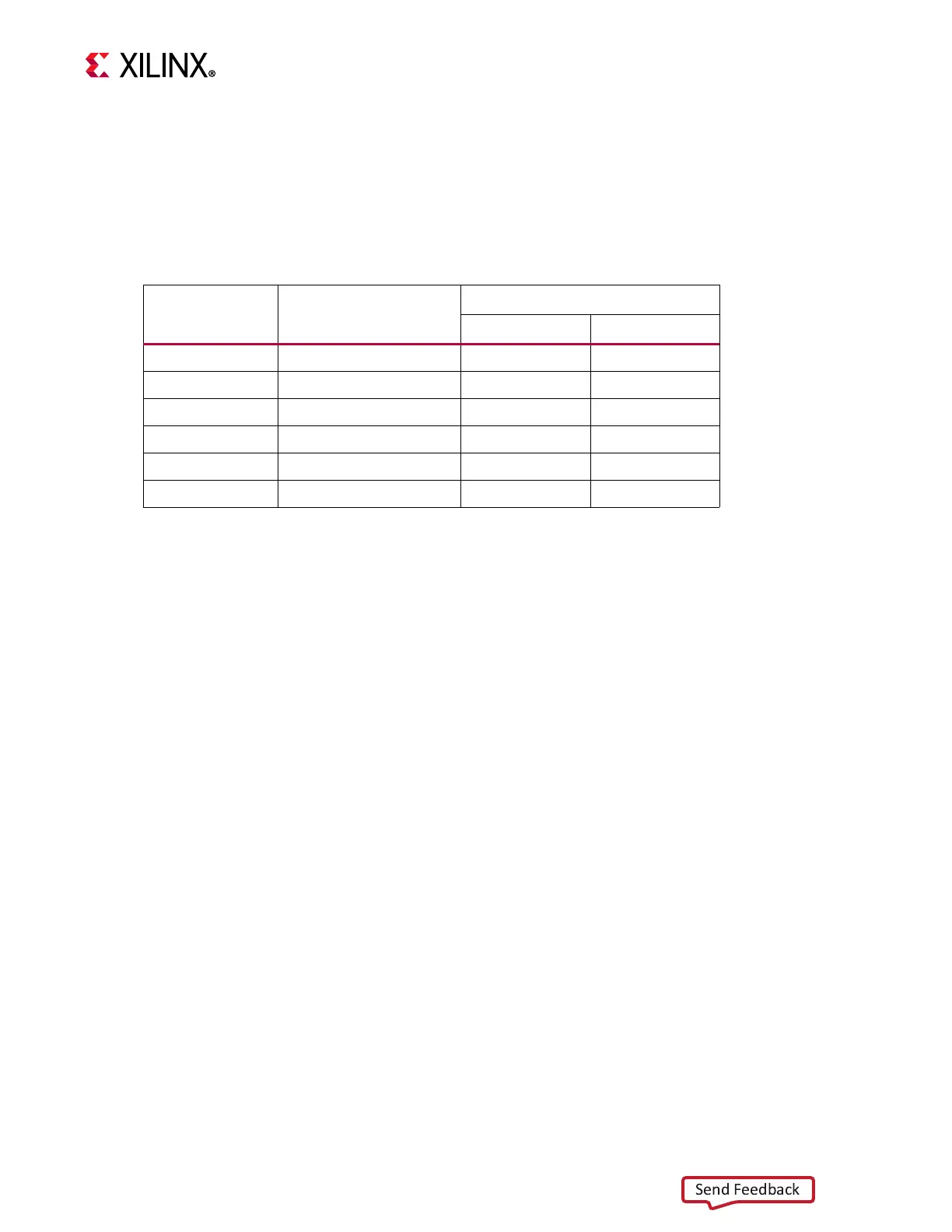
U41. The RFSoC U1 bank 501 and MSP430 U42 pin numbers are listed in Tab l e 3- 11.
Through the I2C0 bus RFSoC MIO pins, the PMU has access to the board power controllers
and power monitors. See Figure 3-3, page 29 for more details.
See the Zynq UltraScale+ Device Technical Reference Manual (UG1085) [Ref 3] for more
details about the PMU interface.
SD1 (MIO 39-51)
A PS-side interface to an SD card connector is provided for booting and file system storage.
This interface is used for the SD boot mode and supports SD3.0 access post boot.
SD Card Interface
[Figure 2-1, callout 6]
The ZCU111 board includes a secure digital input/output (SDIO) interface to provide access
to general purpose non-volatile SDIO memory cards and devices. Information for the SD
I/O card specification can be found at the SanDisk Corporation [Ref 17] or SD Association
[Ref 18] websites. The ZCU111 SD card interface supports the SD1_LS configuration boot
mode documented in the Zynq UltraScale+ Device Technical Reference Manual (UG1085)
[Ref 3].
The SDIO signals are connected to XCZU28DR RFSoC PS bank 501, which has its VCCMIO set
to 1.8V. The six SD interface nets MIOxx_SDIO_DAT[0:3], MIO50_SDIO_CMD, and
MIO51_SDAIO_CLK each have a series 30Ω resistor at the bank 501 source. An NXP
IP4856CX25 SD 3.0-compliant voltage level-translator U107 is present between the
XCZU28DR RFSoC and the SD card connector (J100). The NXP IP4856CX25 U107 device
provides SD3.0 capability with SDR104 performance.
Table 3-11: XCZU28DR U1 to MSP430 Connections
XCZU28DR
(U1) Pin
Net Name
MSP430 U42
Pin Name Pin #
F26 MIO37_PMU_GPO5 P1_0 13
C27 MIO36_PMU_GPO4 P1_1 14
E26 MIO35_PMU_GPO3 P1_2 15
B27 MIO34_PMU_GPO2 P1_3 16
A27 MIO33_PMU_GPO1 P1_4 17
A26 MIO32_PMU_GPO0 P1_5 18