ZCU111 Board User Guide 74
UG1271 (v1.1) August 6, 2018 www.xilinx.com
Chapter 3: Board Component Descriptions
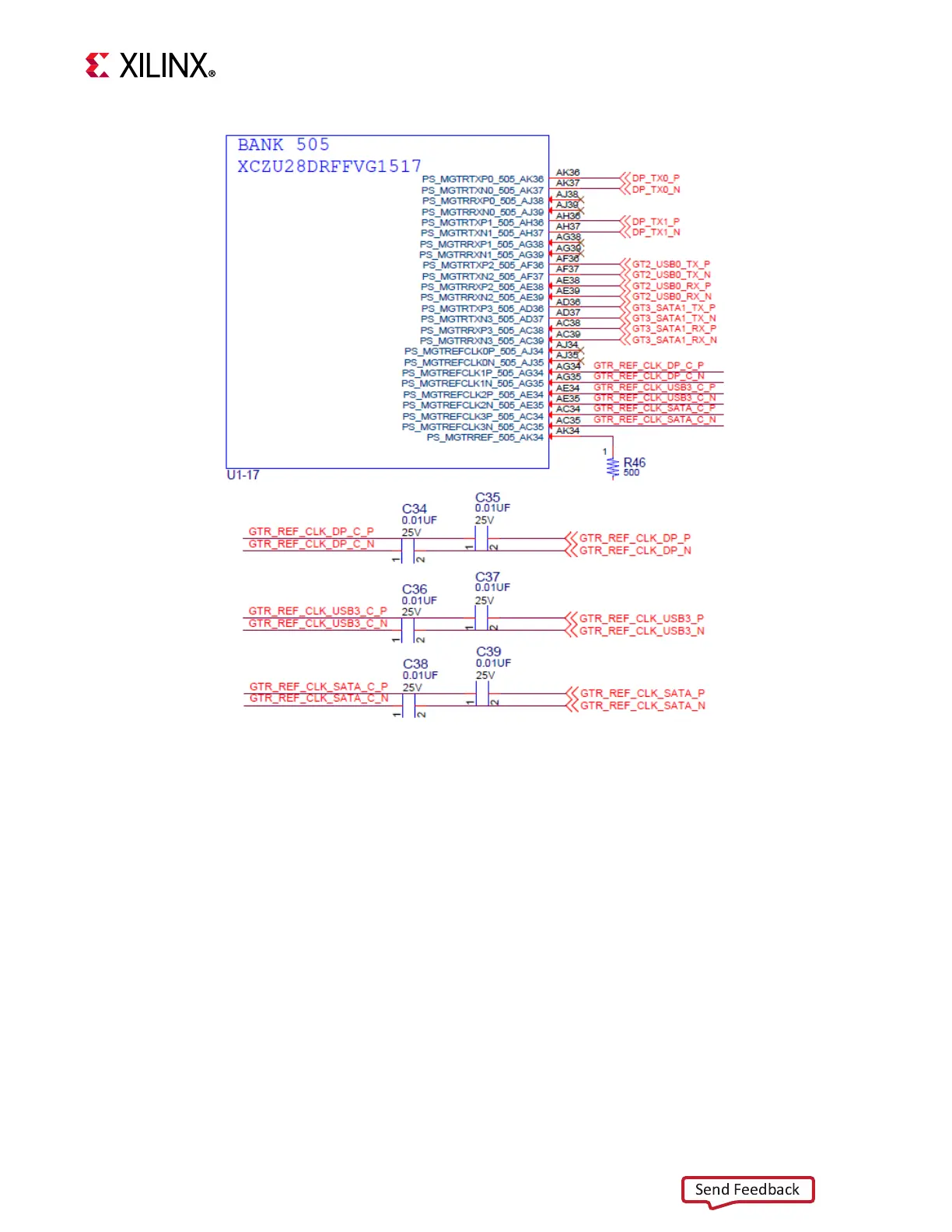
Bank 505 DP (DisplayPort) lanes 0 and 1 TX support the 2-channel source only PS-side
DisplayPort circuitry described in DPAUX (MIO 27-30), page 35.
Bank 505 USB0 lane 2 supports the USB3.0 interface described in USB 3.0 Transceiver and
USB 2.0 ULPI PHY, page 39.
Bank 505 SATA1 lane 3 supports the M.2 SATA connector U170 as shown in Figure 3-31.
Bank 505 reference clocks are connected to the U46 SI5341B clock generator as detailed in
SI5341B 10 Independent Output Any-Frequency Clock Generator, page 47.
Bank 505 connections are referenced in Appendix B, Xilinx Design Constraints.
X-Ref Target - Figure 3-30
Figure 3-30: PS-GTR Lane Assignments