28
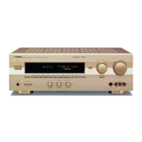
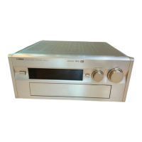
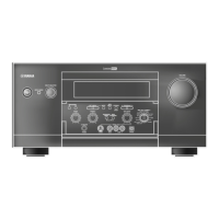
DSP-A595a
IC4 : YSS918D-F (AC3D2av)
DSP + AC-3 (Digital Dolby)/Pro Logic/DTS Digital Surround Decoder
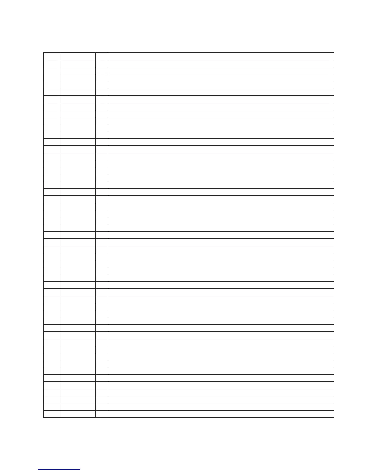
51 VDD2 +3V power supply
52 NONPCM O non-PCM data output terminal, non-PCM data detect
53 CRC O CRC output terminal (normally unconnected)
54 MUTE O Mute output terminal, output data mute detect
55 KARAOKE O Karaoke output terminal (normally unconnected)
56 SURENC O Surround encoder output terminal (normally unconnected)
57 /SDBCK0 O Inverted signal of serial data bit clock output terminal 0 (normally unconnected)
58 RAMA6 O RAM address output terminal 6, connected to external 1M SRAM address
59 RAMA5 O RAM address output terminal 5, connected to external 1M SRAM address
60 VSS Ground
61 RAMA4 O RAM address output terminal 4, connected to external 1M SRAM address
62 /IC I Initial clear input terminal
63 TEST Test terminal (normally unconnected)
64 RAMA3 O RAM address output terminal 3, connected to external 1M SRAM address
65 /CSB I Chip select B input terminal,coefficient and program RAM chip select signal input
66 /CS I Chip select input terminal, microprocessor interface chip select signal input
67 SO O Serial data output terminal, microprocessor interface serial data output
68 SI I Serial data input terminal, microprocessor interface and coefficient and program RAM serial data input
69 SCK I Serial clock intput terminal, microprocessor interface and coefficient and program RAM serial clock input
70 RAMA2 O RAM address output terminal 2, connected to external 1M SRAM address
71 VDD1 +5V power supply
72 RAMD0 I/O RAM data bus terminal 0, connected to external 1M SRAM data
73 RAMD1 I/O RAM data bus terminal 1, connected to external 1M SRAM data
74 RAMD2 I/O RAM data bus terminal 2, connected to external 1M SRAM data
75 RAMD3 I/O RAM data bus terminal 3, connected to external 1M SRAM data
76 RAMD4 I/O RAM data bus terminal 4, connected to external 1M SRAM data
77 RAMD5 I/O RAM data bus terminal 5, connected to external 1M SRAM data
78 RAMD6 I/O RAM data bus terminal 6, connected to external 1M SRAM data
79 RAMD7 I/O RAM data bus terminal 7, connected to external 1M SRAM data
80 VSS Ground
81 VDD2 +3V power supply
82 SDWCK0 I Serial data word clock input terminal 0
83 SDBCK0 I Serial data bit clock input terminal 0
84 SDIA0 I Serial data input A terminal 0, AC-3/DTS bit stream (or PCM) data input
85 SDIA1 I Serial data input A terminal 1 (normally connected to ground)
86 RAMA1 O RAM address output terminal 1, connected to external 1M SRAM address
87 RAMA0 O RAM address output terminal 0, connected to external 1M SRAM address
88 RAMWEN O RAM write enable output terminal, connected to external 1M SRAM write enable
89 RAMOEN O RAM output enable output terminal, connected to external 1M SRAM output enable
90 VSS Ground
91 VDD +3V power supply
92 IPORT7 I Input port terminal 7 (normally connected to ground)
93 IPORT6 I Input port terminal 6 (normally connected to ground)
94 IPORT5 I Input port terminal 5 (normally connected to ground)
95 IPORT4 I Input port terminal 4 (normally connected to ground)
96 IPORT3 I Input port terminal 3 (normally connected to ground)
97 IPORT2 I Input port terminal 2 (normally connected to ground)
98 IPORT1 I Input port terminal 1 (normally connected to ground)
99 IPORT0 I Input port terminal 0 (normally connected to ground)
No. Name I/O Function
100 VSS Ground


 To Next Page