2-2
IM 701610-61E
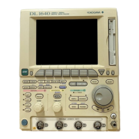
2.2 Connecting the Probe
Input Terminals
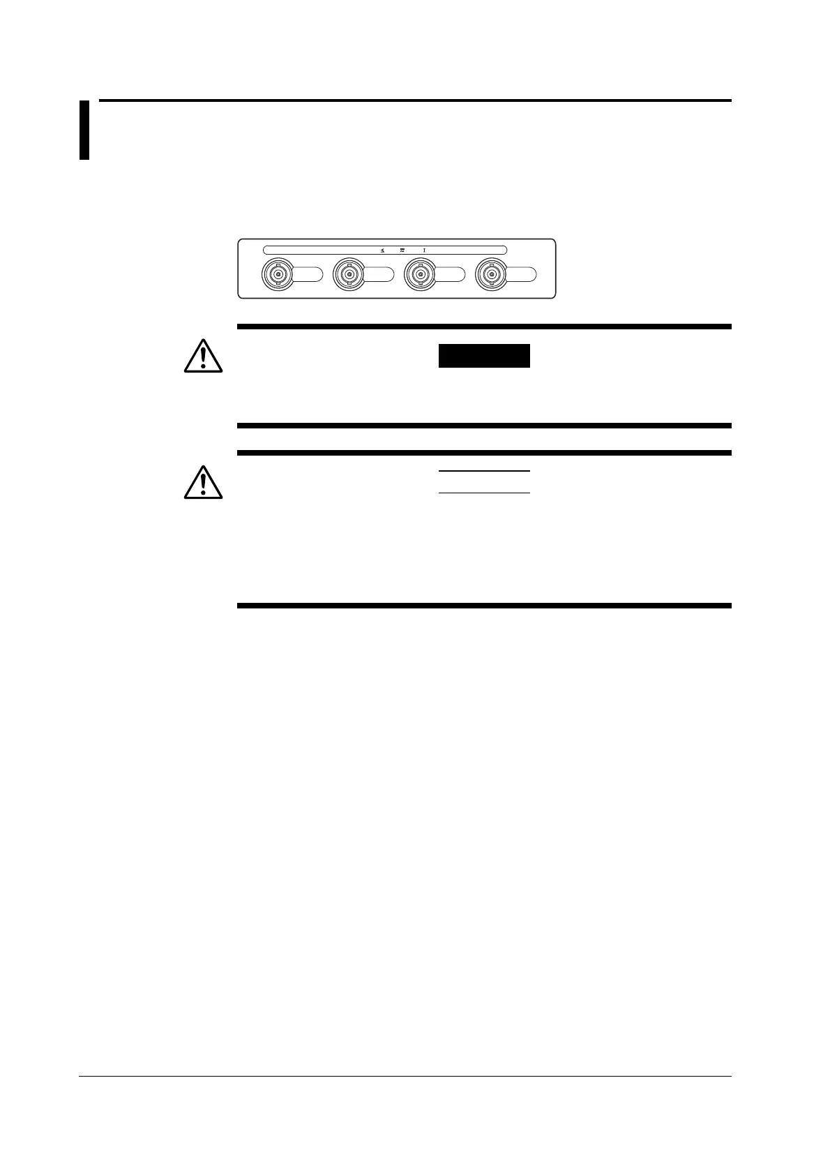
Connect the probe to one of the input terminals located at the lower section of the front
panel. The input impedance is 1 MΩ±1.0% and approximately 28 pF.
CH 1 CH 2 CH 3 CH 4
1MΩ 28pF 300V
CAT
WARNING
To prevent fire or electric shock, do not use this instrument for category
II, III, or IV measurements.
CAUTION
The maximum input voltage for 1 MΩ input is 300 VDC or 300 Vrms
when the frequency is 1 kHz or less. Applying a voltage exceeding this
maximum can damage the input section. If the frequency is above 1
kHz, the input section may be damaged even when the voltage is below
this value.
Precautions to Be Taken When Connecting a Probe
• When performing SPI bus signal analysis, connect the signals to the input terminals
as follows:
CH1: Clock signal
CH2: Data input/output signal (Data1)
*
CH3: Data input/output signal (Data2)
*
CH4: Chip select signal (CS)
* CH2 and CH3 can be connected to either the data input signal or the data output signal. The
DL1640/DL1640L handles the data of the signal connected to CH2 and CH3 as Data1 and
Data2, respectively.
• When connecting a probe to the instrument for the first time, perform phase correction
of the probe as described in section 3.5, “Compensating the Probe (Phase
Correction)” in the
DL1620/DL1640/DL1640L User’s Manual IM 701610-01E
. Failure
to do so may result in unstable gain across different frequencies, thereby preventing
correct measurement. Calibration must be performed for each channel.
• Note that if the object being measured is directly connected to the instrument without
using a probe, correct measurements may not be possible due to loading effects.
 Loading...