MAINTENANCE MANUAL
IFR 6000
2-2-1
Page 6
Aug 1/06
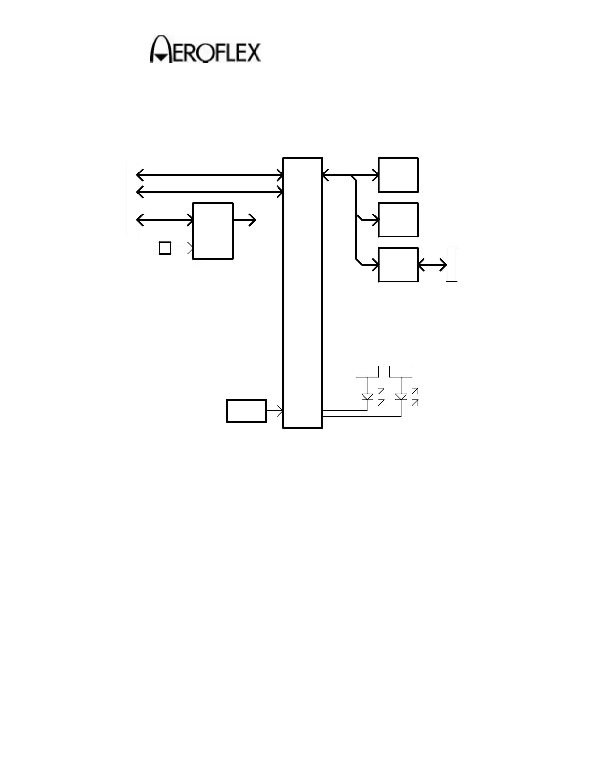
C. Processor PCB Assy
The Processor PCB Assy contains the processor, FLASH, NVRAM, Serial Ports and an
interface bus for controlling the Test Set.
056M-02
RESET
CPLD
OSC
CPLD JTAG PROG
RS-232 DEBUG
BDM
32 MB (2 MB X 16)
16 MB (1 MB X 16)
8 MB (512 kB X 16)
8 MB (256 kB X 32)
NVRAM
I/F
BUS
CPU
FLASH
DATA BUS I/F
+3.3V+3.3V
Processor PCB Assy Block Diagram
Figure 3
(1) CPU
The microprocessor used contains a DRAM controller, DMA controller, interrupt
controller, timers, parallel and serial interfaces and on-chip debug support. The
microprocessor contains 4 kB of cache and 8 kB of on-chip SRAM. The
microprocessor runs at a maximum clock speed of 40 MHz. The Processor PCB Assy
contains a 36.864 MHz oscillator, divided by two within the CPLD, and then provided
to the CPU.
(2) External Memory (FLASH)
The Processor PCB Assy memory arrangement is 256k x 16, 512k x 16, 1M x 16 or
2M x 16.
During reset, the external interrupts are sampled to define the port size and wait-state
generation for chip select CS0 (FLASH). The interrupts are strapped for a 16-bit port
with 15 wait states to allow the start program execution from the FLASH.
 Loading...