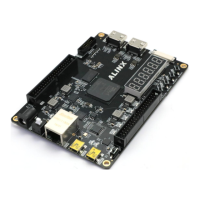
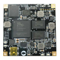
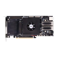
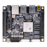
ARTIX-7 FPGA Development Board AX7101 User Manual
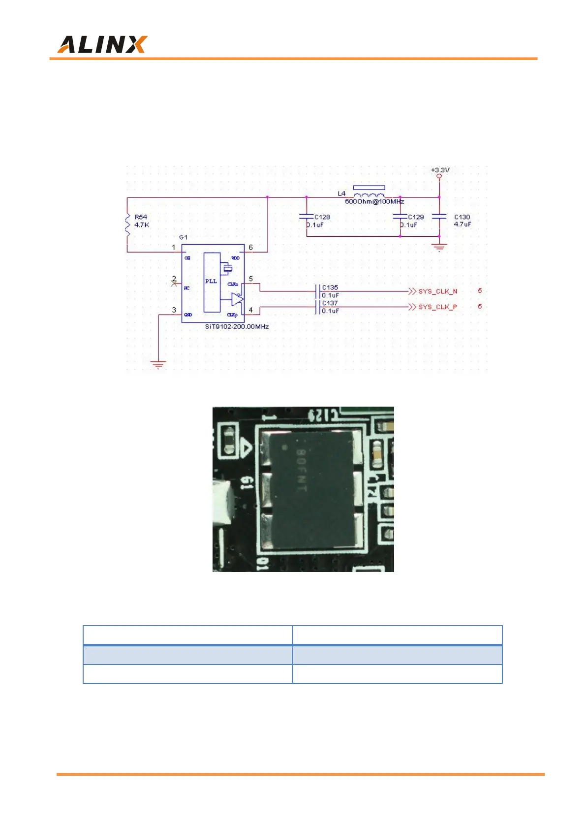
BANK34 global clock pin MRCC (R4 and T4) of the FPGA. This 200Mhz
differential clock can be used to drive the user logic in the FPGA. Users can
configure the PLLs and DCMs inside the FPGA to generate clocks of different
frequencies.
Figure 2-3-1: 200Mhz Active Differential Crystal Schematic
Figure 2-3-2: 200Mhz Active Differential Crystal on the Core Board
200Mhz Differential Clock Pin Assignment
Part 2.3.2: 125Mhz Active Differential Crystal
G2 in Figure 2-3-3 is the 125Mhz active differential crystal, which is the
reference input clock provided to the GTP module inside the FPGA. The crystal


 To Next Page