Check the following voltages at the
diagnostics point while connected to PC.
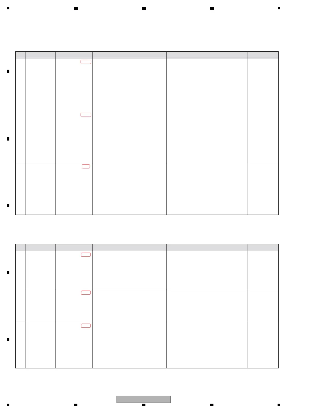
[Power supply of VBUS]
USBA_VBUS/USBB_VBUS
(5 V)
[Data circuit]
USBA_DP, USBA_DM, USBB_DP, USBB_DM
(Not fixed of 0 V)
Check the following voltages at the
diagnostics point while connected to PC.
[Power supply of VBUS]
USBA_VBUS/USBB_VBUS
(5 V)
[Data circuit]
USBA_DP, USBA_DM, USBB_DP, USBB_DM
(Not fixed of 0 V)
—
1 The parts defect
or the mount
defect between
USB/ETHER UCOM
(IC401) and CN1
2 The parts defect
or the mount
defect in
USBB Assy
MAIN Assy
CN1
2 pin
(USBA_VBUS)
7 pin
(USBB_VBUS)
CN1
3 pin, 4 pin
(USBA_DP/USBA_DM)
8 pin, 9 pin
(USBB_DP/DM)
USBB Assy
CN3101
2 pin
(USBA_VBUS)
7 pin
(USBB_VBUS)
CN3101
3 pin, 4 pin
(USBA_DP/USBA_DM)
8 pin, 9 pin
(USBB_DP/USBB_DM)
USBB Assy
JA3101
1 pin
(USBA_VBUS)
2 pin, 3 pin
(USBA_DP/USBA_DM)
JA3102
1 pin
(USBB_VBUS)
2 pin, 3 pin
(USBB_DP/USBB_DM)
[9] USBA/USBB
[9-1] USBA/USBB does not recognize the unit
Step Cause Diagnostics Point Item to be Checked Corrective Action Reference
6.2 CROSSFADER
CALIBRATION
6.2 CROSSFADER
CALIBRATION
! If the voltage is confirmed correctly, go to
step 2.
! If not, the wire or the USBB Assy may be
defective.
Replace its.
!
If the voltage is confirmed correctly, perform
a crosscheck of
Assy and replace the defective
Assy.
! If not, confirm the parts between CN3101 and
JA3101, and between CN3101 and JA3102.
Replace the defective parts.
Check the following voltages at the
diagnostics point.
[Power supply of MULTI I/O circuit]
V+5R2D_VBUS (5.2 V)
V+12M (12 V)
Check the following voltages at the
diagnostics point while connected to PC.
[Power supply control of MULTI I/O circuit]
USBPSW_FA (3.3 V)
USBPSW_EN (3.3 V)
1 Power defect of
MULTI I/O circuit
2 Power supply
control of
MULTI I/O circuit
USBA Assy
JA3051
1 pin
(V+5R2D_VBUS)
USBP Assy
CN3151
5 pin
(V+12M)
USBP Assy
IC3152
8 pin
(USBPSW_FA)
IC3152
4 pin
(USBPSW_EN)
[10] MULTI I/O
[10-1] A connected device does not recognize the unit
Step Cause Diagnostics Point Item to be Checked Corrective Action Reference
! If the voltage is confirmed correctly, go to
step 2.
! If not, the parts on the circuit around IC3151
and IC3152 of USBP Assy may be defective.
Replace its.
! If the voltage is confirmed correctly, go to
step 3.
! If not the USBPSW_FA/USBPSW_EN circuit
may be defective. Check for the status of
soldering and replace it.
9-1-1-1
9-1-1-2
9-1-2
10-1-1
10-1-2
Check the following voltages at the
diagnostics point while connected to PC.
[The signal circuit of MULTI I/O circuit]
USBC_DP/USBC_DM
(Not fixed of 0 V)
3 The signal circuit
defect of
MULTI I/O circuit
USBA Assy
JA3051
2 pin, 3 pin
(USBC_DP/USBC_DM)
MAIN Assy
L1701
1 pin, 4 pin
(USBC_DP/USBC_DM)
! If the voltage is confirmed correctly, perform
a crosscheck of Assy and replace the
defective Assy.
! If not, the circuit or the parts may be defective
in the following places.
- Between IC1101 and CN14
- Between CN3051 and JA3051
If the parts other than IC1101 are defective,
replace its. If IC1101 is defective, replace
MAIN Assy.
10-1-3
 Loading...