4–4 Chapter 4: Development Board Setup
Factory Default Switch and Jumper Settings
Cyclone V SoC Development Kit May 2013 Altera Corporation
User Guide
3. Set the DIP switch bank (SW4) to match Table 4–3 and Figure 4–1.
In the following table, up and down indicates the position of the switch with the
board orientation as shown in Figure 4–1.
3 MSEL2
Switch 3 has the following options:
■ ON (up) = MSEL2 is 0.
■ OFF (down) = MSEL2 is 1.
ON
4 MSEL3
Switch 4 has the following options:
■ ON (up) = MSEL3 is 0.
■ OFF (down) = MSEL3 is 1.
ON
5 MSEL4
Switch 5 has the following options:
■ ON (up) = MSEL4 is 0.
■ OFF (down) = MSEL4 is 1.
ON
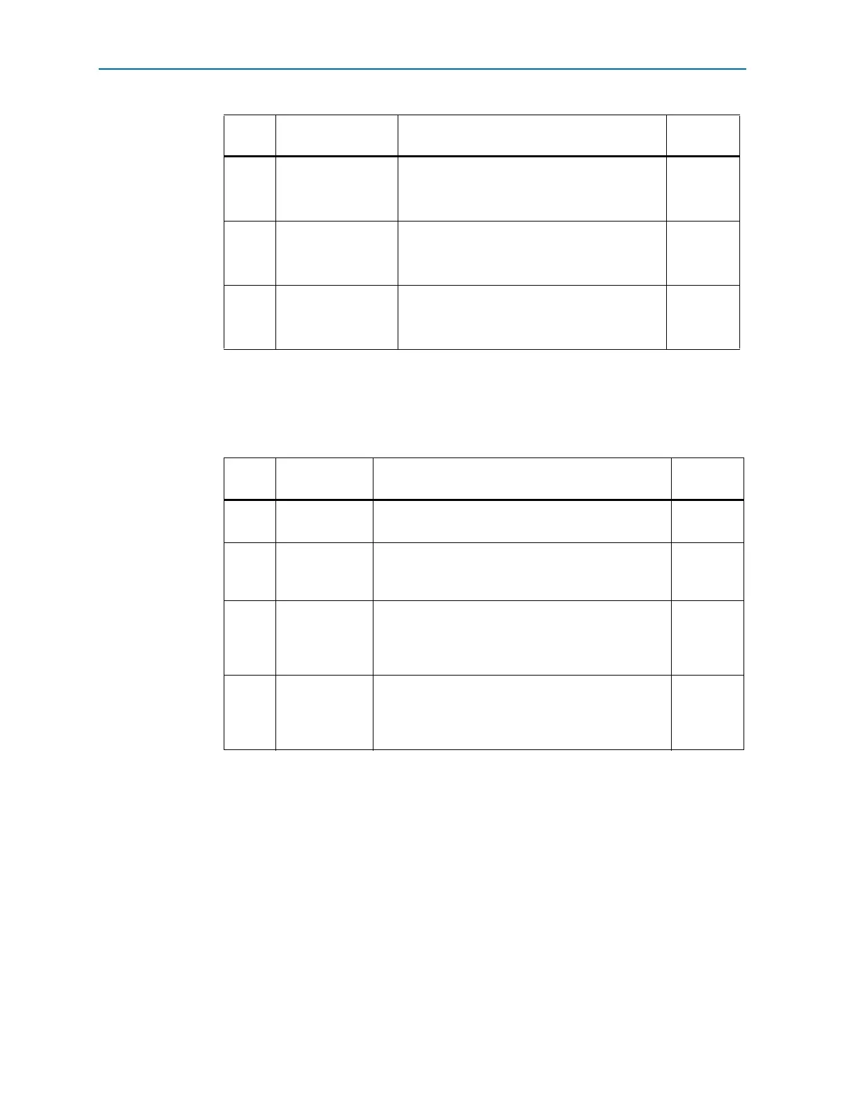
Table 4–3. SW4 JTAG DIP Switch Settings
Switch
Board
Label
Function
Default
Position
1HPS
■ ON (up) = Do not Include HPS in the JTAG chain.
■ OFF (down) = Include HPS in the JTAG chain
OFF
2FPGA
■ ON (up) = Do not Include the FPGA in the JTAG
chain.
■ OFF (down) = Include the FPGA in the JTAG chain.
OFF
3HSMC
■ ON (up) = Do not include the HSMC connector in the
JTAG chain.
■ OFF (down) = Include the HSMC connector in the
JTAG chain.
ON
4MAX
■ ON (up) = Do not include the MAX V system
controller in the JTAG chain.
■ OFF (down) = Include the MAX V system controller in
the JTAG chain.
OFF
Table 4–2. SW3 DIP Switch Settings (Part 2 of 2)
Switch
Board
Label
Function
Default
Position