UG-1308 EVAL-ADuCM355QSPZ Evaluation Board
Rev. A | Page 20 of 24
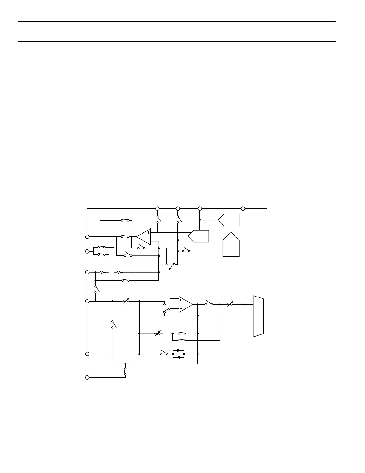
LOW POWER TIA0/TIA1 GAIN RESISTOR
CALIBRATION
The ADuCM355 contains two independent, low power
TIA channels.
Each TIA has an independent, programmable gain resistor to
scale the input current from the SE0 pin and the SE1 pin to a
voltage that the ADC can measure.
Figure 36 shows the gain resistor for the low power TIA0. A
similar diagram is valid to use for the low power TIA1.
Similar to the example described in the High Speed TIA Gain
Resistor Calibration section, adjust the gain resistor to convert
the current from the SE0 input pin and the SE1 input pin to a
differential voltage across the R
TIA
resistors.
These resistors have an initial accuracy range and vary with
temperature, as specified in the ADuCM355 data sheet.
When these resistors are uncalibrated, an error is present when
measuring an absolute input current.
To generate a precision calibration current, use the low power
DAC to create a differential voltage across an external precision
R
CAL
resistor that is connected to the ADuCM355 RCAL0 pin
and RCAL1 pin. The precision calibration current is routed
through either the low power TIA0 gain resistor or the low
power TIA1 gain resistor.
Because the calibration current value is known and the ADC
can measure the voltage drop across each R
TIA
resistor, the exact
R
TIA
resistor value can be determined.
Figure 37 and Figure 38 show the setup and switch settings
used to connect the low power DAC outputs to the external
R
CAL
resistor so that the current flows into the LPTIAx gain
resistors, LPRTIAx.
Several example projects in the ADuCM355 SDK implement a
function to calibrate the gain resistor. For further details on
how to use this function, visit
https://wiki.analog.com/resources/eval/user-guides/eval-
ad5940/calibration_routines/lptia_cal?doc=EVAL-
ADuCM355QSPZ-UG-1308.PDF.
BIAS0
SW12
SW6
PA
SW9
LPTIA0_P_LPF0
ADC
MUX
SW7
LPTIA
FORCE/SENSE
SW0
SW1
LPTIACON0
[12:10]
LPTIACON0
[9:5]
PROGRAMMABLE
GAIN RESISTOR
SW2
SW8
SW14
SW15
SW4
RE0
SW10
SW3
SW11
10kΩ 10kΩ
RE0
SW5
CE0
CAP_POT0
SE0
RC0_0
RC0_1
SW13
ZERO0
REF2V5
LPDAC0
ULPBUF
ULPREF
TO
CHANNEL 1
IN4/LPF0
R
LPF
ULPTIACON0
[15:13]
R
TIA
R
LOAD
16887-027
Figure 36. LPTIA0 Gain Calibration Resistor

 Loading...


