FIGURES
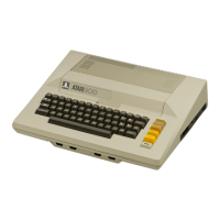
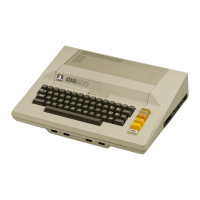
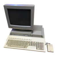
Figure 1-1. The ATARI 400/800 Computer Consoles 1-2
Figure 1-2. Sample Notice of Changes Page 1-5
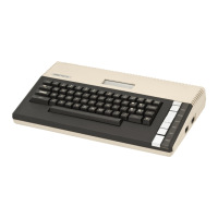
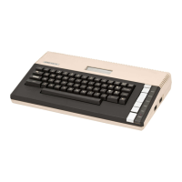
Figure 1-3. ATARI 400/800 Computer Console Systems 1-8
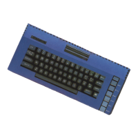
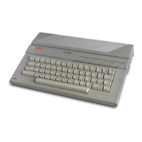
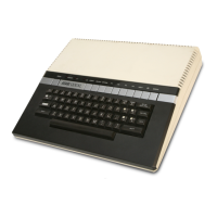
Figure 1-4. ATARI 400 Computer Console, Side View 1-9
Figure 1-5. ATARI 800 Computer Console, Side View 1-10
Figure 2-1. Conversion to 300 Ohm Antenna Input Impedance 2-3
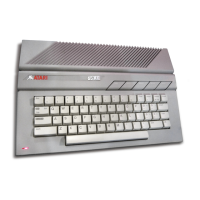
Figure 2-2. ATARI 400/800 Computer Consoles, Side View 2-5
Figure 2-3. 400/800 Consoles, Cartridge Door Open 2-6
Figure 2-4. ATARI Disk Drive Cable Connections 2-8
Figure 2-5. ATARI 40 Column Printer Cable Connections 2-9
Figure 2-6. ATARI 850 Interface Module Cable Diagram 2-10
Figure 3-1. The ATARI Keyboard 3-3
Figure 3-2. Special Graphics Using the CTRL Key 3-4
Figure 3-3. Special Graphics Using the ESC Key 3-5
Figure 3-4. SHIFT Keyboard and Key Combination 3-6
Figure 4-1. Major Functional Modules of the ATARI 400/800 4-18
Figure 4-2. Block Diagram of the CPU Board 4-19
Figure 4-3. Schematic Diagram of the CPU Board 4-20
Figure 4-4. Atari 400 motherboard Block Diagram 4-21
Figure 4-5a. Atari 400 motherboard schematic part 1 4-22
Figure 4-5b. Atari 400 motherboard schematic part 2 4-23
Figure 4-6. Pin Assignments of ATARI Custom Chips POKEY,
ANTIC and CTIA 4-24
Figure 4-7. Block Diagram of the Motherboard Console System (800) 4-27
Figure 4-8a. Schematic Diagram of Motherboard Console System(800) 4-28
Figure 4-8b. Schematic Diagram of Motherboard Console System(800) 4-29
Figure 4-9. Block Diagram of the ROM Personality Board 4-30
Figure 4-10. Schematic Diagram of the ROM Personality Board 4-31
Figure 4-11. Block Diagram of the RAM Board (8K) 4-32
Figure 4-12. Schematic Diagram of the RAM Board (8K) 4-33
Figure 4-13. Block Diagram of the RAM Board (16K) 4-34
Figure 4-14. Schematic Diagram of the RAM Board (16K) 4-35
Figure 4-15. Block Diagram of the Power Supply (400) 4-36
Figure 4-16. Schematic Diagram of the Power Supply (400) 4-37
Figure 4-17. Block Diagram of the Power Supply (800) 4-38
Figure 4-18. Schematic Diagram of the Power Supply (800) 4-39
Figure 4-19. Block Diagram of a Program Cartridge 4-40
Figure 4-20. Schematic Diagram of a Program Cartridge 4-41
Figure 5-1. System Check-Out Flowchart 5-4
Figure 5-2. Stand Alone Test Special Tools 5-8
Figure 5-3. Any Video Test Screen Display 5-10
Figure 5-4. Graybar Test Screen Display 5-11
Figure 5-5. Color Bar Test Screen Display 5-12
Figure 5-6.400 Console Color Adjustment 5-13
Figure 5-7. 800 Console Color Adjustment 5-14
Figure 5-8. RAM Test Matrix Screen Display 5-15
Figure 5-9. PORT Test Error Table Screen Display 5-17
Figure 5-10. 400 Console, Assembled Without Casting 5-20
Figure 5-11. 800 Console, Assembled Without Casting 5-21
Figure 5-12. RAM Memory Board Locations, 8K 5-24
Figure 5-13. RAM Memory Board Locations, 16K 5-25
Figure 5-14. CPU Printed Circuit Board, Locations 5-26
Figure 5-15. 400 Console Motherboard, Locations 5-28
Figure 5-16. 800 Console Motherboard, Locations 5-29