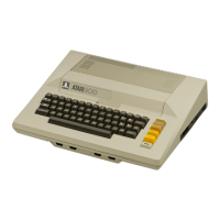
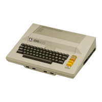
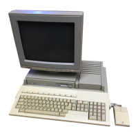
4.3.1 Central Processing Unit Board (CPU Board)
The Central Processing Unit (CPU) pcb contains the 6502 CPU (or MPU)
CHIP (A303), the CTIA chip (A301), the ANTIC chip (A302), tri-state
address buffers (Z303 & Z304), and the Clock Generator (Z302A and
Z302B). See Figures 4-2 and 4-3.
CPU 6502 Integrated Circuit. The 6502 microprocessor contains
registers flags, interconnections, arithmetic logic, and control
logic which recognize operation codes. The salient characteristics of
the 6502 microprocessor are summarized as follows:
• Byte-oriented structure
• 151 opcodesDecimal or binary arithmetic modes
• Seven addressing modes
• True indexing
• Stack pointer
• Two interrupt levels
• 64K address range
• Integral clock circuit
• Single 5-volt dc power requirement
Figure 4-3 shows pin assignment of the 6502 microprocessor. The
functions of the pins are given below.
AB0-AB15 Address Bus. The Address Bus signals on the 6502 MPU are
push-pull drivers capable of driving one standard TTL load and 130
picofarads of capacitance. The address placed on the Address Bus is
determined by the Program Counter in the 6502 MPU or a stored address
in RAM memory, specified by the program instruction. The ANTIC chip
also puts addresses on the system Address Bus, sharing control of the
bus with the 6502 MPU.
DB0-DB7 Data Bus. Pins 26 through 33 are connected to the
bidirectional Data Bus. Each of these pins is connected to both an
input and an output buffer. The output buffer is in three-state high
impedance (isolated)
condition except when data transfer out takes place. All data
transfers take place during the Phase 2 clock pulse. During Phase 1
the Data Bus is in the isolated high impedance condition. The Data
Bus output buffer is a push-pull driver, like the Address Bus driver,
and is capable of driving a TTL load. The data on this bus from an
external support chip must be stable before the end of the Phase 2
clock pulse.
ATARI Personal Computers 4-5