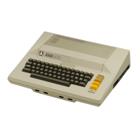
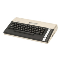
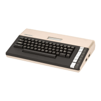
The POKEY integrated circuit provides the interface between the
Keyboard, Serial I/O ports, and the microprocessor. Also contained
within the chip are four semi-independent audio channels, each with
its own f requency, noise, and volume control. Figure 4-6 shows pin
assignments of the POKEY chip, and the functions of the pins are
given below.
D0 - D7 Data Bus. The Data Bus lines (8 bits) are used to input and
output information between the POKEY chip and the microprocessor. The
Data Bus lines are routed to the processor through bidirectional
tristate buffers.
CS0 Chip Select. This signal originates on the ROM Personality pcb,
and is used by the microprocessor to select the POKEY chip. The POKEY
chip is selected when this line goes low.
AUD Audio Signąl. Four sound registers are located in the POKEY chip.
The output of these registers are used to develop the audio signal.
A0 - A3 Address Bus. These address lines are used in conjunction with
the Chip Select (CS0) line to address parts of the POKEY chip.
KR2. This input line is held low during the selection of certain
keys. The keys that take this line to an active low are the Break,
Control, and both shift keys.
KR1. This line goes low to indicate that a key has been found
depressed during a Keyboard scan. The value on pins K0 - K5 when KR1
goes low is sent to the microprocessor to determine the key
depressed.
K0 - K5. The value on these pins increments as the Keyboard is
scanned.
The value indicates a Keyboard key position.
P0 - P7. Two lines correspond to each of the four connector ports on
the front of the Console. Each line is an analog input into the POKEY
chip which converts this analog signal into an eight-bit binary code.
R/W - Read/Write. When R/W goes low (logic0) data is transferred from
the microprocessor Write operation) to the POKEY chip. When R/W goes
high (logic 1) data is transferred from the POKEY chip (Read
operation) to the microprocessor.
Ph 2 or Φ2 - Clock Input. Phase 2 of Master Clock is used by the
Pokey chip to generate its own internal timing.
SID - Serial Input Data. Serial Data from devices such as the Program
Recorder and the Floppy Disk Drive are input on this line.
SOD - Serial Output Data. Data is output serially to peripheral
devices on this line.
4-8 System Service Manual
Clocks OCLK and BCLK. These clocks are used as timing control signals
for the input and output of data.