13
8025I–AVR–02/09
ATmega48P/88P/168P/328P
4.5.1 SPH and SPL – Stack Pointer High and Stack Pointer Low Register
4.6 Instruction Execution Timing
This section describes the general access timing concepts for instruction execution. The AVR
CPU is driven by the CPU clock clk
CPU
, directly generated from the selected clock source for the
chip. No internal clock division is used.
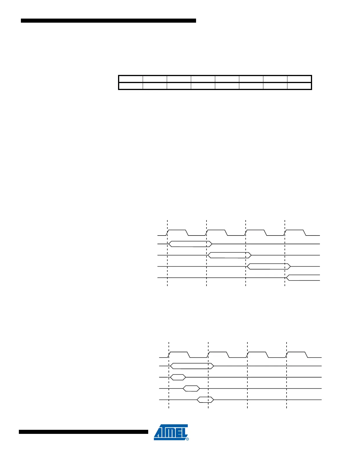
Figure 4-4 shows the parallel instruction fetches and instruction executions enabled by the Har-
vard architecture and the fast-access Register File concept. This is the basic pipelining concept
to obtain up to 1 MIPS per MHz with the corresponding unique results for functions per cost,
functions per clocks, and functions per power-unit.
Figure 4-4. The Parallel Instruction Fetches and Instruction Executions
Figure 4-5 shows the internal timing concept for the Register File. In a single clock cycle an ALU
operation using two register operands is executed, and the result is stored back to the destina-
tion register.
Figure 4-5. Single Cycle ALU Operation
Bit 151413121110 9 8
0x3E (0x5E) SP15 SP14 SP13 SP12 SP11 SP10 SP9 SP8 SPH
0x3D (0x5D) SP7 SP6 SP5 SP4 SP3 SP2 SP1 SP0 SPL
76543210
Read/Write R/W R/W R/W R/W R/W R/W R/W R/W
R/W R/W R/W R/W R/W R/W R/W R/W
Initial Value
RAMEND RAMEND RAMEND RAMEND RAMEND RAMEND RAMEND RAMEND
RAMEND RAMEND RAMEND RAMEND RAMEND RAMEND RAMEND RAMEND
clk
1st Instruction Fetch
1st Instruction Execute
2nd Instruction Fetch
2nd Instruction Execute
3rd Instruction Fetch
3rd Instruction Execute
4th Instruction Fetch
T1 T2 T3 T4
CPU
Total Execution Time
Register Operands Fetch
ALU Operation Execute
Result Write Back
T1 T2 T3 T4
clk
CPU