308
8025I–AVR–02/09
ATmega48P/88P/168P/328P
25.7.14 Reading the Calibration Byte
The algorithm for reading the Calibration byte is as follows (refer to ”Programming the Flash” on
page 302 for details on Command and Address loading):
1. A: Load Command “0000 1000”.
2. B: Load Address Low Byte, 0x00.
3. Set OE
to “0”, and BS1 to “1”. The Calibration byte can now be read at DATA.
4. Set OE
to “1”.
25.7.15 Parallel Programming Characteristics
For chracteristics of the Parallel Programming, see ”Parallel Programming Characteristics” on
page 326.
25.8 Serial Downloading
Both the Flash and EEPROM memory arrays can be programmed using the serial SPI bus while
RESET
is pulled to GND. The serial interface consists of pins SCK, MOSI (input) and MISO (out-
put). After RESET
is set low, the Programming Enable instruction needs to be executed first
before program/erase operations can be executed. NOTE, in Table 25-17 on page 309, the pin
mapping for SPI programming is listed. Not all parts use the SPI pins dedicated for the internal
SPI interface.
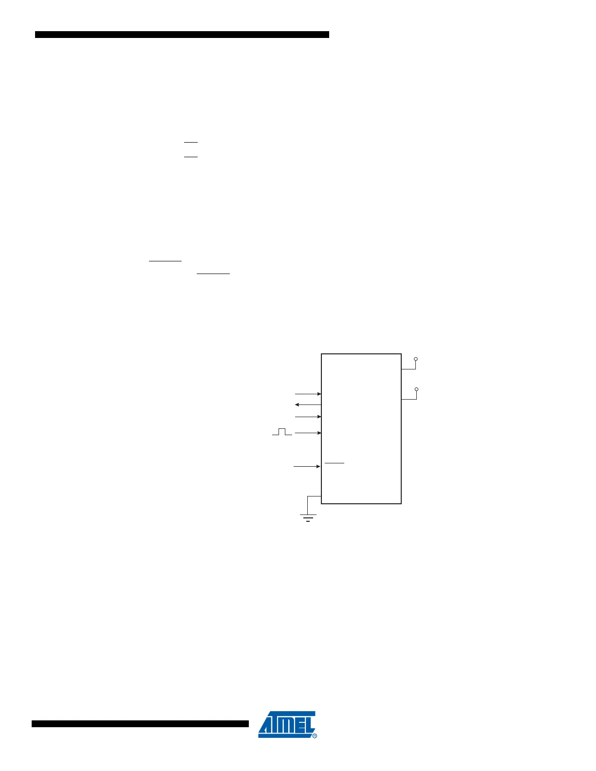
Figure 25-7. Serial Programming and Verify
(1)
Notes: 1. If the device is clocked by the internal Oscillator, it is no need to connect a clock source to the
XTAL1 pin.
2. V
CC
- 0.3V < AV
CC
< V
CC
+ 0.3V, however, AV
CC
should always be within 1.8 - 5.5V
When programming the EEPROM, an auto-erase cycle is built into the self-timed programming
operation (in the Serial mode ONLY) and there is no need to first execute the Chip Erase
instruction. The Chip Erase operation turns the content of every memory location in both the
Program and EEPROM arrays into 0xFF.
Depending on CKSEL Fuses, a valid clock must be present. The minimum low and high periods
for the serial clock (SCK) input are defined as follows:
Low: > 2 CPU clock cycles for f
ck
< 12 MHz, 3 CPU clock cycles for f
ck
>= 12 MHz
High: > 2 CPU clock cycles for f
ck
< 12 MHz, 3 CPU clock cycles for f
ck
>= 12 MHz
VCC
GND
XTAL1
SCK
MISO
MOSI
RESET
+1.8 - 5.5V
AVCC
+1.8 - 5.5V
(2)