141
8025I–AVR–02/09
ATmega48P/88P/168P/328P
14. Timer/Counter0 and Timer/Counter1 Prescalers
”8-bit Timer/Counter0 with PWM” on page 94 and ”16-bit Timer/Counter1 with PWM” on page
113 share the same prescaler module, but the Timer/Counters can have different prescaler set-
tings. The description below applies to both Timer/Counter1 and Timer/Counter0.
14.1 Internal Clock Source
The Timer/Counter can be clocked directly by the system clock (by setting the CSn2:0 = 1). This
provides the fastest operation, with a maximum Timer/Counter clock frequency equal to system
clock frequency (f
CLK_I/O
). Alternatively, one of four taps from the prescaler can be used as a
clock source. The prescaled clock has a frequency of either f
CLK_I/O
/8, f
CLK_I/O
/64, f
CLK_I/O
/256, or
f
CLK_I/O
/1024.
14.2 Prescaler Reset
The prescaler is free running, i.e., operates independently of the Clock Select logic of the
Timer/Counter, and it is shared by Timer/Counter1 and Timer/Counter0. Since the prescaler is
not affected by the Timer/Counter’s clock select, the state of the prescaler will have implications
for situations where a prescaled clock is used. One example of prescaling artifacts occurs when
the timer is enabled and clocked by the prescaler (6 > CSn2:0 > 1). The number of system clock
cycles from when the timer is enabled to the first count occurs can be from 1 to N+1 system
clock cycles, where N equals the prescaler divisor (8, 64, 256, or 1024).
It is possible to use the prescaler reset for synchronizing the Timer/Counter to program execu-
tion. However, care must be taken if the other Timer/Counter that shares the same prescaler
also uses prescaling. A prescaler reset will affect the prescaler period for all Timer/Counters it is
connected to.
14.3 External Clock Source
An external clock source applied to the T1/T0 pin can be used as Timer/Counter clock
(clk
T1
/clk
T0
). The T1/T0 pin is sampled once every system clock cycle by the pin synchronization
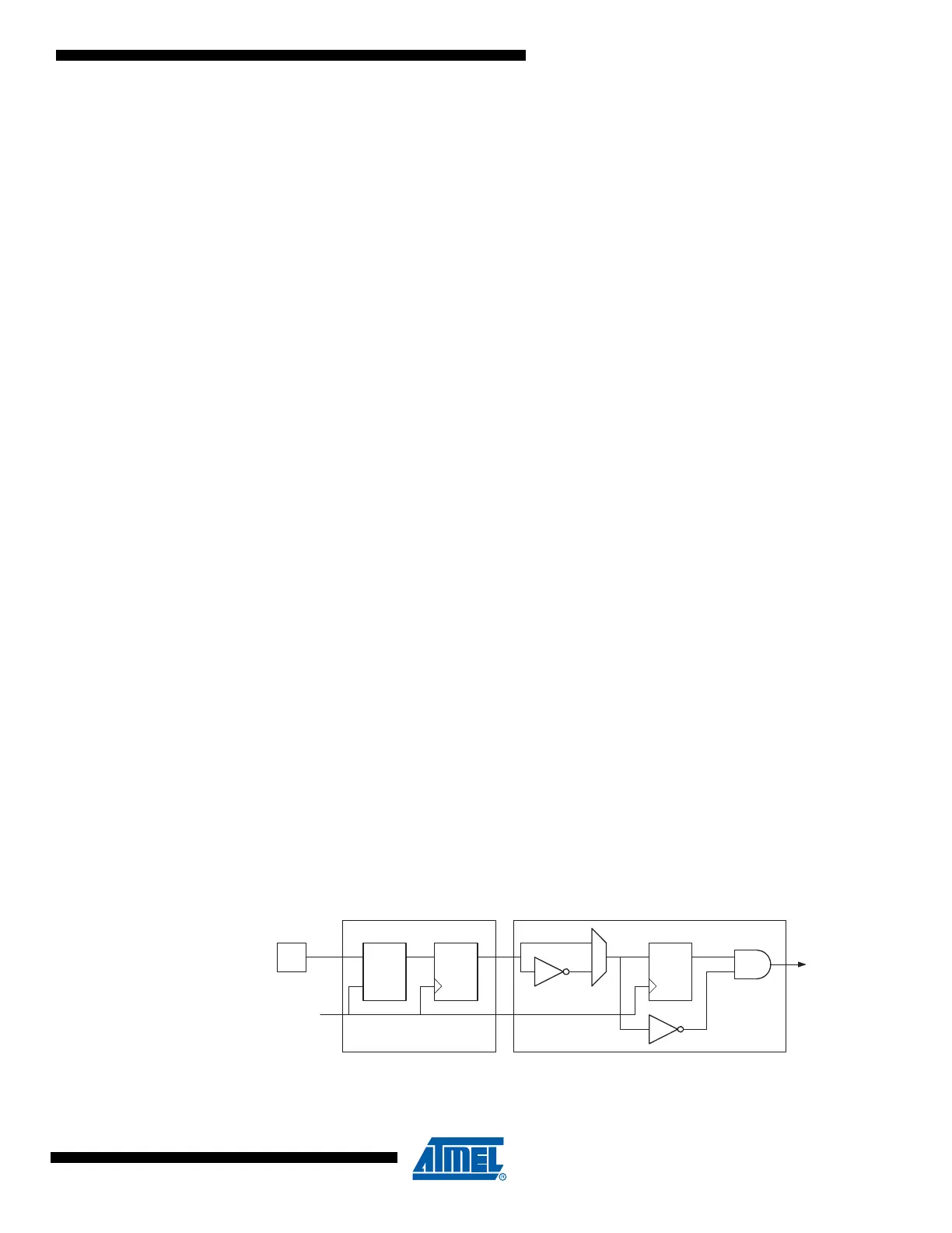
logic. The synchronized (sampled) signal is then passed through the edge detector. Figure 14-1
shows a functional equivalent block diagram of the T1/T0 synchronization and edge detector
logic. The registers are clocked at the positive edge of the internal system clock (
clk
I/O
). The latch
is transparent in the high period of the internal system clock.
The edge detector generates one clk
T1
/clk
T
0
pulse for each positive (CSn2:0 = 7) or negative
(CSn2:0 = 6) edge it detects.
Figure 14-1. T1/T0 Pin Sampling
The synchronization and edge detector logic introduces a delay of 2.5 to 3.5 system clock cycles
from an edge has been applied to the T1/T0 pin to the counter is updated.
Tn_sync
(To Clock
Select Logic)
Edge DetectorSynchronization
DQDQ
LE
DQ
Tn
clk
I/O