177
8025I–AVR–02/09
ATmega48P/88P/168P/328P
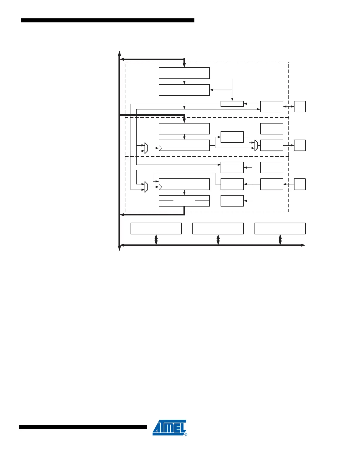
Figure 17-1. USART Block Diagram
(1)
Note: 1. Refer to Figure 1-1 on page 2 and Table 11-9 on page 88 for USART0 pin placement.
17.3 Clock Generation
The Clock Generation logic generates the base clock for the Transmitter and Receiver. The
USART supports four modes of clock operation: Normal asynchronous, Double Speed asyn-
chronous, Master synchronous and Slave synchronous mode. The UMSELn bit in USART
Control and Status Register C (UCSRnC) selects between asynchronous and synchronous
operation. Double Speed (asynchronous mode only) is controlled by the U2Xn found in the
UCSRnA Register. When using synchronous mode (UMSELn = 1), the Data Direction Register
for the XCKn pin (DDR_XCKn) controls whether the clock source is internal (Master mode) or
external (Slave mode). The XCKn pin is only active when using synchronous mode.
PARITY
GENERATOR
UBRRn [H:L]
UDRn(Transmit)
UCSRnA UCSRnB UCSRnC
BAUD RATE GENERATOR
TRANSMIT SHIFT REGISTER
RECEIVE SHIFT REGISTER RxDn
TxDn
PIN
CONTROL
UDRn (Receive)
PIN
CONTROL
XCKn
DATA
RECOVERY
CLOCK
RECOVERY
PIN
CONTROL
TX
CONTROL
RX
CONTROL
PARITY
CHECKER
DATA BUS
OSC
SYNC LOGIC
Clock Generator
Transmitter
Receiver