321
8025I–AVR–02/09
ATmega48P/88P/168P/328P
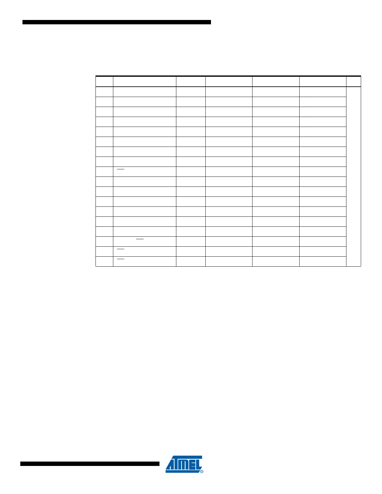
26.6 SPI Timing Characteristics
See Figure 26-5 and Figure 26-6 for details.
Note: 1. In SPI Programming mode the minimum SCK high/low period is:
- 2 t
CLCL
for f
CK
< 12 MHz
- 3 t
CLCL
for f
CK
> 12 MHz
2. All DC Characteristics contained in this datasheet are based on simulation and characteriza-
tion of other AVR microcontrollers manufactured in the same process technology. These
values are preliminary values representing design targets, and will be updated after character-
ization of actual silicon.
Table 26-5. SPI Timing Parameters
Description Mode Min Typ Max
1 SCK period Master See Table 16-5
ns
2 SCK high/low Master 50% duty cycle
3 Rise/Fall time Master 3.6
4 Setup Master 10
5Hold Master 10
6 Out to SCK Master 0.5 • t
sck
7 SCK to out Master 10
8 SCK to out high Master 10
9SS
low to out Slave 15
10 SCK period Slave 4 • t
ck
11 SCK high/low
(1)
Slave 2 • t
ck
12 Rise/Fall time Slave 1600
13 Setup Slave 10
14 Hold Slave t
ck
15 SCK to out Slave 15
16 SCK to SS high Slave 20
17 SS
high to tri-state Slave 10
18 SS low to SCK Slave 20