143
7598H–AVR–07/09
ATtiny25/45/85
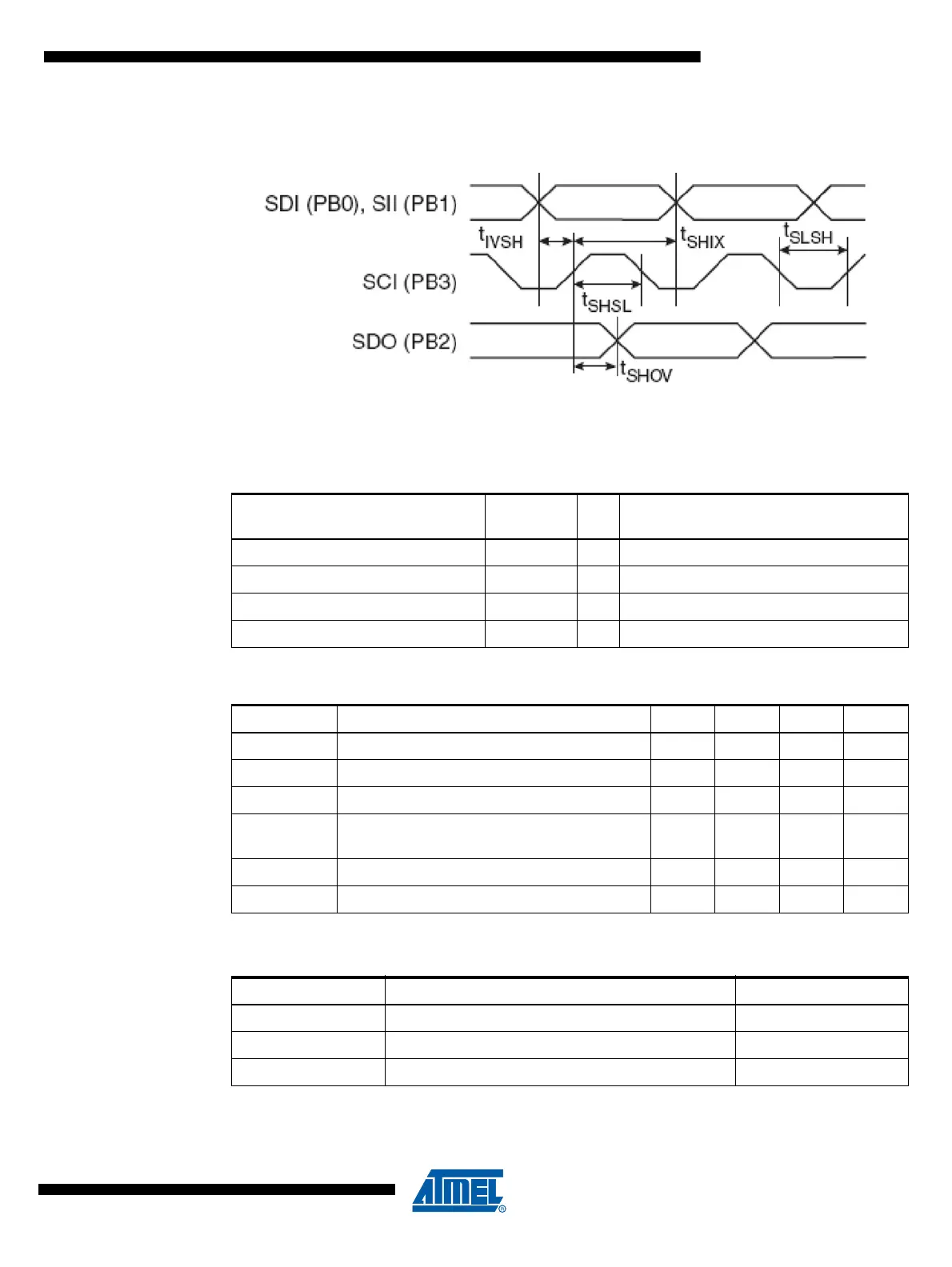
Figure 21-4. High-voltage Serial Programming
Table 21-12. Pin Name Mapping
Signal Name in High-voltage
Serial Programming Mode Pin Name I/O Function
SDI PB0 I Serial Data Input
SII PB1 I Serial Instruction Input
SDO PB2 O Serial Data Output
SCI PB3 I Serial Clock Input (min. 220ns period)
Table 21-13. High-voltage Serial Programming Characteristics T
A
= 25°C ±10%,
V
CC = 5.0V ±10% (Unless otherwise noted)
Symbol Parameter Min Typ Max Units
t
SHSL SCI (PB3) Pulse Width High 125 ns
t
SLSH SCI (PB3) Pulse Width Low 125 ns
t
IVSH SDI (PB0), SII (PB1) Valid to SCI (PB3) High 50 ns
tSHIX
SDI (PB0), SII (PB1) Hold after SCI (PB3)
High
50 ns
t
SHOV SCI (PB3) High to SDO (PB2) Valid 16 ns
t
WLWH_PFB Wait after Instr. 3 for Write Fuse Bits 2.5 ms
Table 21-14. Pin Values Used to Enter Programming Mode
Pin Symbol Value
SDI Prog_enable[0] 0
SII Prog_enable[1] 0
SDO Prog_enable[2] 0